

Method for producing monocrystalline n-silicon solar cells, as well as a solar cell produced according to such a method
a technology of solar cells and monocrystalline n-silicon, which is applied in the field of producing monocrystalline n-silicon solar cells, and a solar cell produced according to such a method, can solve the problems of low efficiency, large surface recombination rate, and inability to passivate the emitter with local contacts, so as to avoid the disadvantages of the related art and high productivity
- Summary
- Abstract
- Description
- Claims
- Application Information
AI Technical Summary
Benefits of technology
Problems solved by technology
Method used
Image

Examples
Embodiment Construction
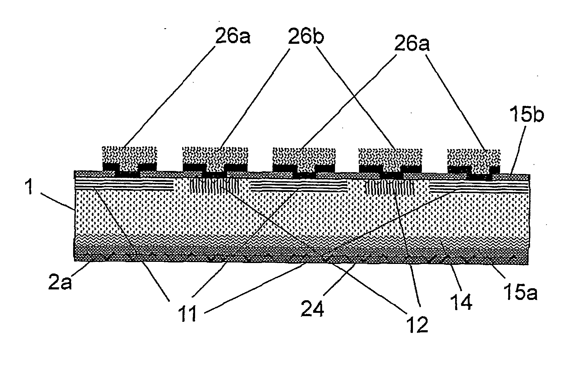
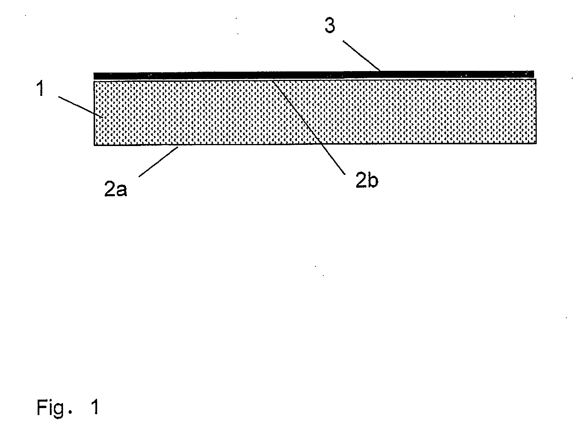
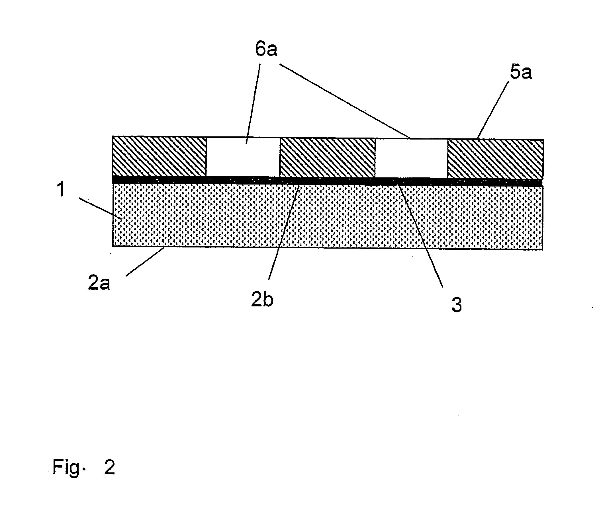
[0052]In a first method step according to FIG. 1, entire rear side 2b of n-silicon wafer 1, which is untextured in the illustrated example, is covered by an aluminum or aluminum-containing layer 3, which forms the emitter dopant. The front side of the wafer is denoted by reference numeral 2a, and the rear side by reference numeral 2b.
[0053]In a further step, aluminum-containing layer 3 is brought into contact with a shadow mask 5a and structured by a dry-etching step in plasma 7a containing chlorine gas (cf. FIGS. 2 and 3).
[0054]As an alternative, an organic mask layer may be applied as well, e.g., by so-called ink-jetting, and the aluminum in the regions that have remained free then be etched in a wet-chemical manner.
[0055]The two discussed technological variants produce longitudinal openings 4 in the form of strips in the region of breakthroughs 6a of mask 5a.
[0056]At a later point, the BSF doping material is diffused into strip-shaped openings 4 in aluminum layer 3 at a lateral...
PUM
 Abstract
Description
Claims
Application Information