Optically testing chiplets in display device

a display device and chiplet technology, applied in the field of display devices, can solve the problems of low performance, low manufacturing process efficiency, and large size of thin-film transistors made from amorphous or polycrystalline silicon, and achieve the effect of improving the performance of control elements and efficient way to test chiplets

Active Publication Date: 2011-02-24
GLOBAL OLED TECH
View PDF30 Cites 33 Cited by
  • Summary
  • Abstract
  • Description
  • Claims
  • Application Information

AI Technical Summary

Benefits of technology

[0024]The present invention has the advantage that it improves the performance of control elements in a flat-panel substrate and provides an efficient way to test chiplets and electrical connections. The invention is particularly useful during fabrication of OLED devices including chiplets to ensure that the chiplets are operating properly prior to the fabrication of the OLED layers in the device.

Problems solved by technology

Thin-film transistors made from amorphous or polycrystalline silicon are relatively larger and have lower performance than conventional transistors made from crystalline silicon wafers.
Moreover, such thin-film devices typically exhibit local or large-area non-uniformity that results in perceptible non-uniformity in a display employing such materials.
While improvements in manufacturing and materials processes are made, the manufacturing processes are expensive and thin-film device performance continues to be lower than the performance of crystalline silicon devices.
However, there is no teaching of improving the aperture ratio of a display, reducing the cost of such pixel-control devices in cooperation with a display device, or testing the pixel-control devices.
In particular, displays with many pixels (e.g. high-definition televisions) can take a long time to sequentially test each pixel.

Method used


Image

  • Optically testing chiplets in display device
  • Optically testing chiplets in display device
  • Optically testing chiplets in display device

Examples


Embodiment Construction

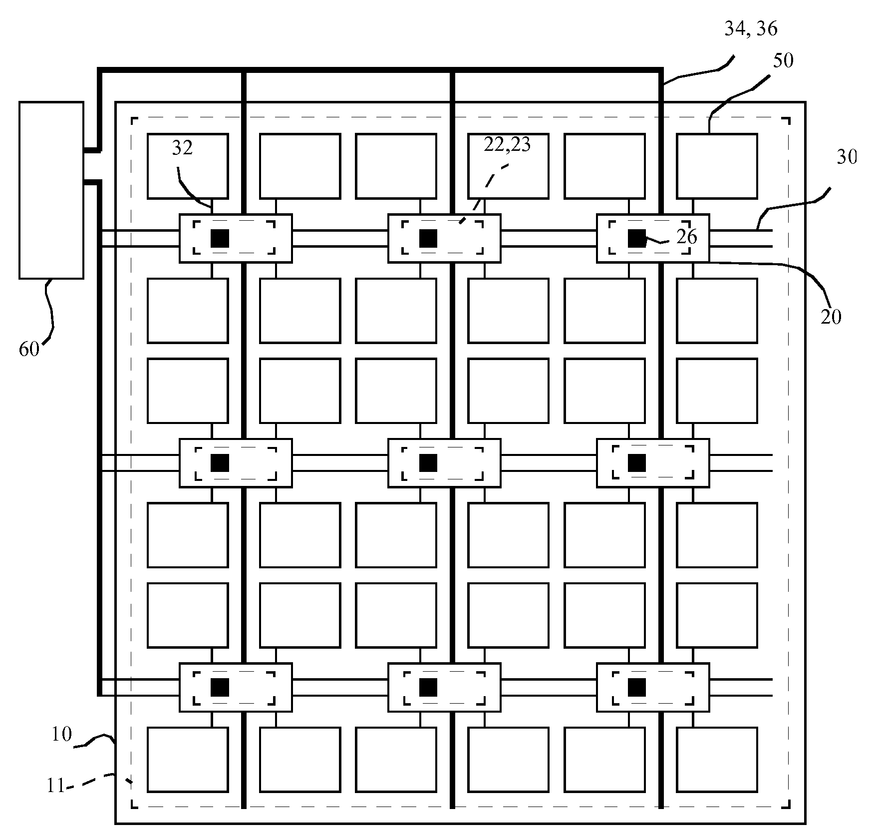
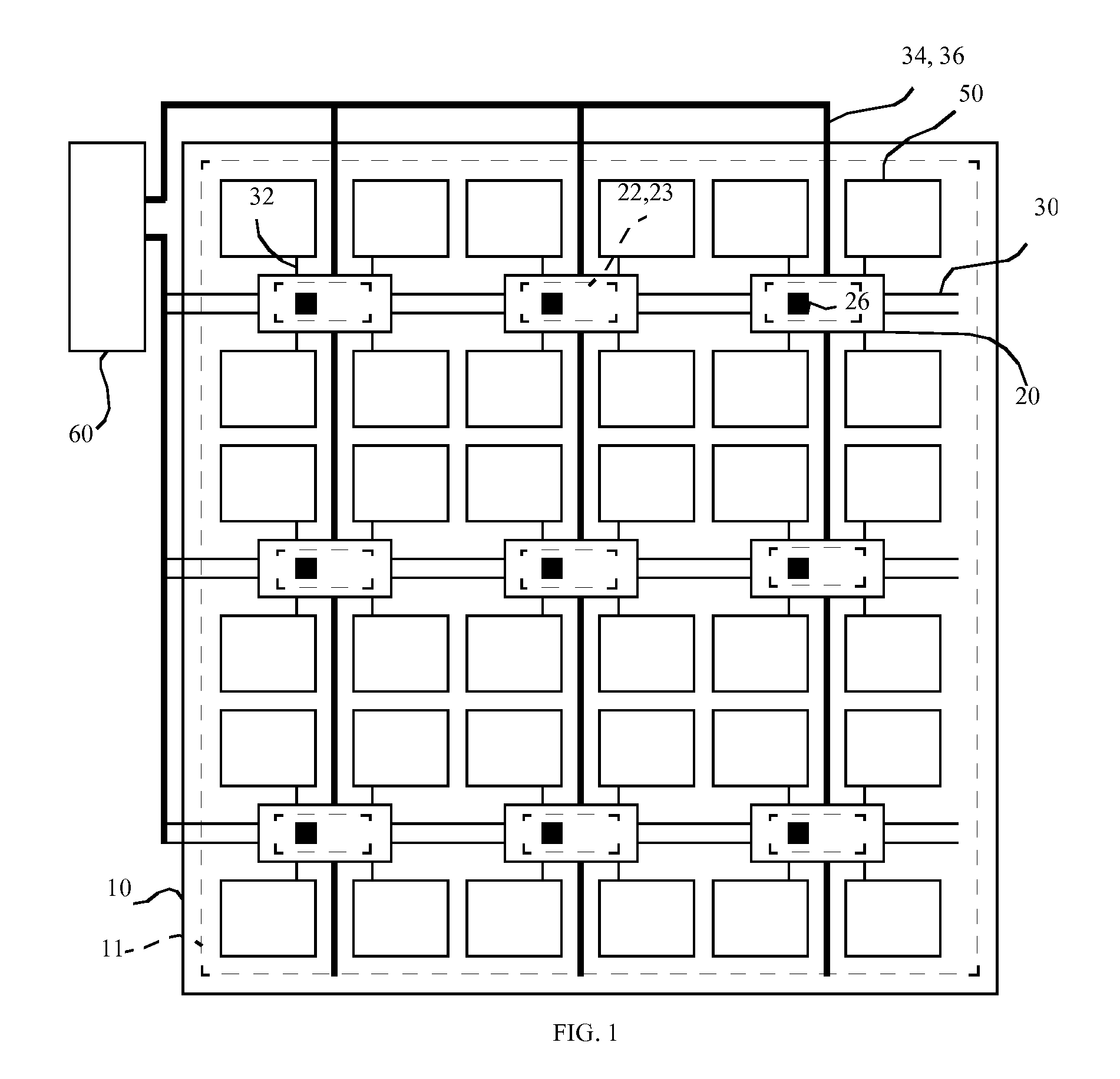
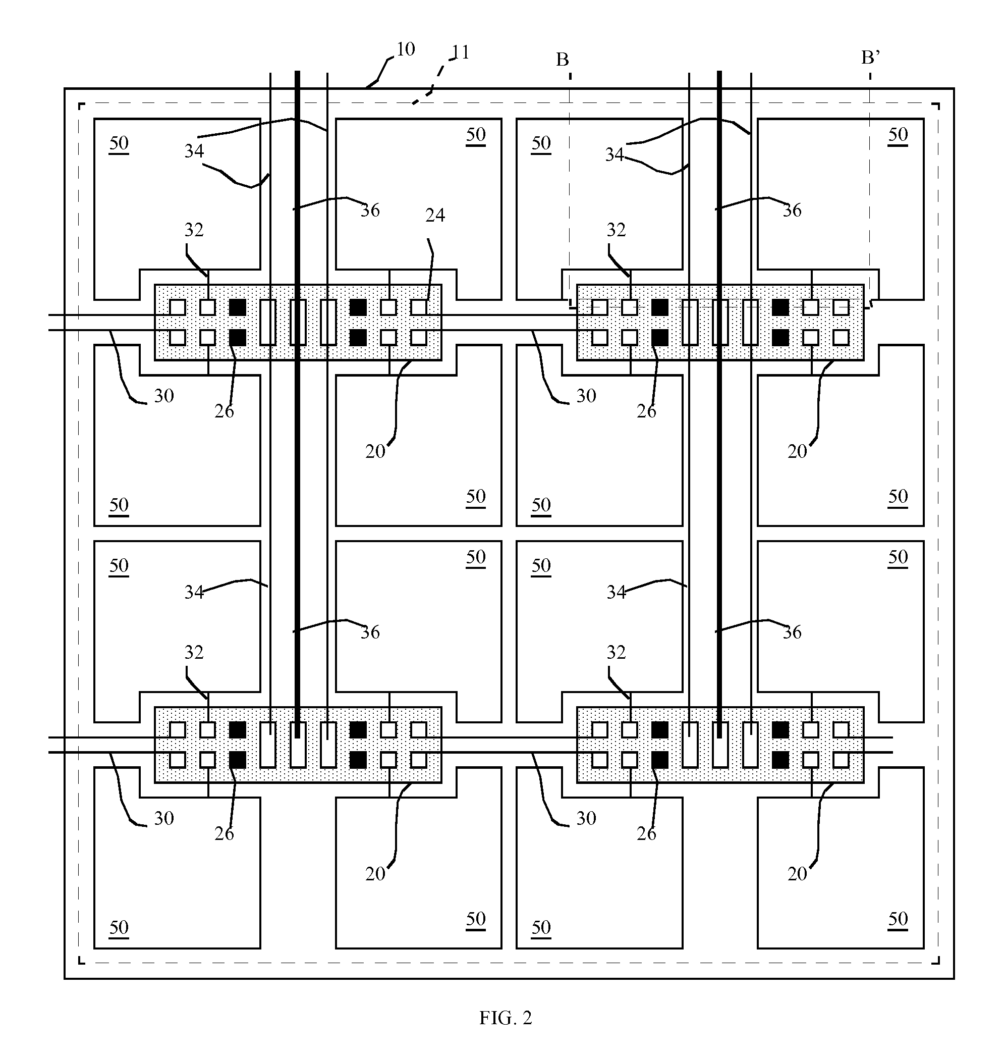
[0036]Referring to schematic FIG. 1 and cross-section FIG. 8, a display, according to one embodiment of the present invention, includes a display substrate 10 having a display area 11. A plurality of pixels 50 are located in the display area 11, each pixel 50 including a control electrode 12, a second electrode 16, and at least one layer of light-emitting material 14 located between the control electrode 12 and second electrode 16 that emits light in response to a current provided by the control electrode 12 and the second electrode 16. A plurality of chiplets 20 having a chiplet substrate 28 independent of the display substrate 10 are located over the display substrate 10 in the display area 11, each chiplet 20 having at least one connection pad 24, at least one pixel control circuit 22, and at least one pixel test circuit 23. The pixel control circuit 22 is connected to the control electrode 12 through an electrical connection 32 for driving the control electrode 12 and the layer ...


PUM


Abstract

A method of making a display includes providing a display substrate having a plurality of control electrodes in a display area; locating a plurality of chiplets responsive to a controller to provide current to the control electrodes, each chiplet having a separate substrate, at least one pixel connection pad electrically connected to a control electrode, and one or more test light emitters formed in the chiplet responsive to the current provided on the control electrodes to emit light; controlling the chiplets to pass current through one or more of the test light emitters formed in the chiplet to emit light; detecting the light emitted by the test light emitters to determine faulty chiplets or chiplet interconnections; replacing or repairing the faulty chiplets or chiplet interconnections; and forming an organic light emitting diode over the substrate in the display area connected to the control electrodes.

Description

CROSS REFERENCE TO RELATED APPLICATION[0001]Reference is made to commonly-assigned U.S. patent application Ser. No. 12 / 191,478 filed Aug. 14, 2008, entitled “OLED Device With Embedded Chip Driving” by Dustin L. Winters et al, the disclosure of which is incorporated herein.FIELD OF THE INVENTION[0002]The present invention relates to display devices having a substrate with distributed, independent chiplet control elements and optically testing such chiplets.BACKGROUND OF THE INVENTION[0003]Flat-panel display devices are widely used in conjunction with computing devices, in portable devices, and for entertainment devices such as televisions. Such displays typically employ a plurality of pixels distributed over a substrate to display images. Each pixel incorporates several, differently colored light-emitting elements commonly referred to as sub-pixels, typically emitting red, green, and blue light, to represent each image element. Pixels and sub-pixels are not distinguished herein; all ...

Claims


Application Information

Patent Timeline
Patent Type & Authority Applications(United States)
IPC IPC(8): G09G5/00G09G3/30H01J9/50
CPCG09G3/006G09G3/2085H01L27/3276G09G2330/12H01L27/3255G09G3/3208H10K59/129H10K59/131H10K71/70G01R31/308
Inventor COK, RONALD S.HAMER, JOHN W.MATTERN, MICHAEL W.
Owner GLOBAL OLED TECH
Why Eureka
Try Eureka