Method of manufacturing a light-emitting diode

a manufacturing method and light-emitting diode technology, applied in semiconductor/solid-state device manufacturing, semiconductor devices, electrical equipment, etc., can solve the problems of deterioration of deterioration of the white light, and drawback of the white light when lighting, so as to improve the general performance of the device over time, the effect of emission properties and higher production costs

Inactive Publication Date: 2011-02-24
CENT NAT DE LA RECHERCHE SCI
View PDF32 Cites 6 Cited by
  • Summary
  • Abstract
  • Description
  • Claims
  • Application Information

AI Technical Summary

Benefits of technology

[0006]A second aim of the present invention is thus to avoid the variation of the colour emission as a function of the intensity of the current of the diode. In the field of non monolithic diodes, white diodes are widely used, which are composed of a first monolithic part emitting in the blue (blue diode), above which a phosphorescent material is positioned which absorbs a part of the blue photons emitted by the blue diode and reemits yellow photons, the combination of such two lights giving a white light.
[0007]However, such two-part diodes of the standard blue diode-phosphor type have, on the one hand, the drawback that the phosphor positioned above the blue diode results in a deterioration of the general performances of the device over time. This leads to a deterioration of the white light over time and to a limitation of the life of the white LED with respect to a standard blue LED. On the other hand, it should be noted that the manufacturing of such a white LED requires a first conventional step of epitaxial growth of the blue LED and an additional step of the deposition of phosphor. Such additional step of the deposition thus involves higher production costs.
[0008]Another aim of the present invention is thus to provide a white diode through epitaxial growth only, i.e. a monolithic diode. Another aim of the present invention is thus to provide a white diode, the emission properties of which are stable over time.
[0011]Another aim of the invention is to provide a diode which can potentially emit in the whole visible spectrum and more particularly when it is excited by a blue LED. At least one of these aims is reached according to the present invention by a device comprising a matrix made of III-V nitride, said matrix comprising at least an active first portion through which an electric current passes and at least a passive second portion through which no electric current passes, said matrix comprising at least a first zone comprising a first stack of quantum wells or planes of quantum dots of III-V nitride, said first zone being positioned in said active first portion and at least a second zone comprising a second stack of quantum wells or planes of quantum dots of III-V nitride, characterised in that said second zone is positioned in said passive portion of said matrix. Thanks to the stacks of quantum wells or quantum dots respectively positioned in the active portion and the passive portion of the device, it is possible to control efficiently the lights emitted by the first zone and the second zone in order to generate, at the device output, a light which can spread on the whole visible spectrum.
[0013]The optical pumping of the second zone in the passive portion of the matrix of the device thus makes it possible to avoid the drawbacks connected to the electric pumping, and more particularly the dependence of the emission on the current intensity. Besides, the monolithic constitution of the matrix comprising the passive zone and the active zone in one III-V nitride material, makes it possible to obtain the device according to the invention with only one step of epitaxial growth. The distribution of the III-V nitride elements in the matrix is carried out according to the invention, so that said first zone forms a quantum confinement and that the second zone forms a quantum confinement, i.e. the part of the matrix between such zones forms a quantum gate between such zones. This is obtained, in a manner known per se, by selecting the III-V nitride materials as a function of the bandgaps of such materials.
[0016]According to another embodiment, which makes it possible to improve the colour temperature and the colour rendering index while obtaining a white light at the device output, said at least one second zone is able to emit photons in the green and in the red by an optical pumping by said photons emitted by said first zone. According to an alternative solution of the invention, said first zone is composed of a stack of quantum wells of the InGaN / GaN type. In such embodiment of the invention, said second zone is composed of a stack of planes of quantum dots of the GaN / AlN type. In order to allow the passage of the current towards the first active zone while making the quantum confinement of the first active zone, said matrix made of III-V nitride includes a third conductive portion which forms a quantum gate for said first zone.

Problems solved by technology

This characteristic may be useful if diodes which can change colours are desired, but it is a drawback for the emission in the white when the purpose is lighting.
However, such two-part diodes of the standard blue diode-phosphor type have, on the one hand, the drawback that the phosphor positioned above the blue diode results in a deterioration of the general performances of the device over time.
This leads to a deterioration of the white light over time and to a limitation of the life of the white LED with respect to a standard blue LED.
Such additional step of the deposition thus involves higher production costs.
It is also known that in such layers, the emission is caused by deep levels resulting from crystalline defects.
The quantum efficiency of this type of layer is thus limited.
The diode of the above-mentioned document does not make it possible to obtain a diode which can emit in the whole visible spectrum by combining the colours between the light emitted in the active zone and the light emitted in the passive zone.
Such a diode thus does not make it possible to make colour combinations between the light emitted by the active zone and the light emitted by the passive zone.

Method used


Image

  • Method of manufacturing a light-emitting diode
  • Method of manufacturing a light-emitting diode
  • Method of manufacturing a light-emitting diode

Examples


Embodiment Construction

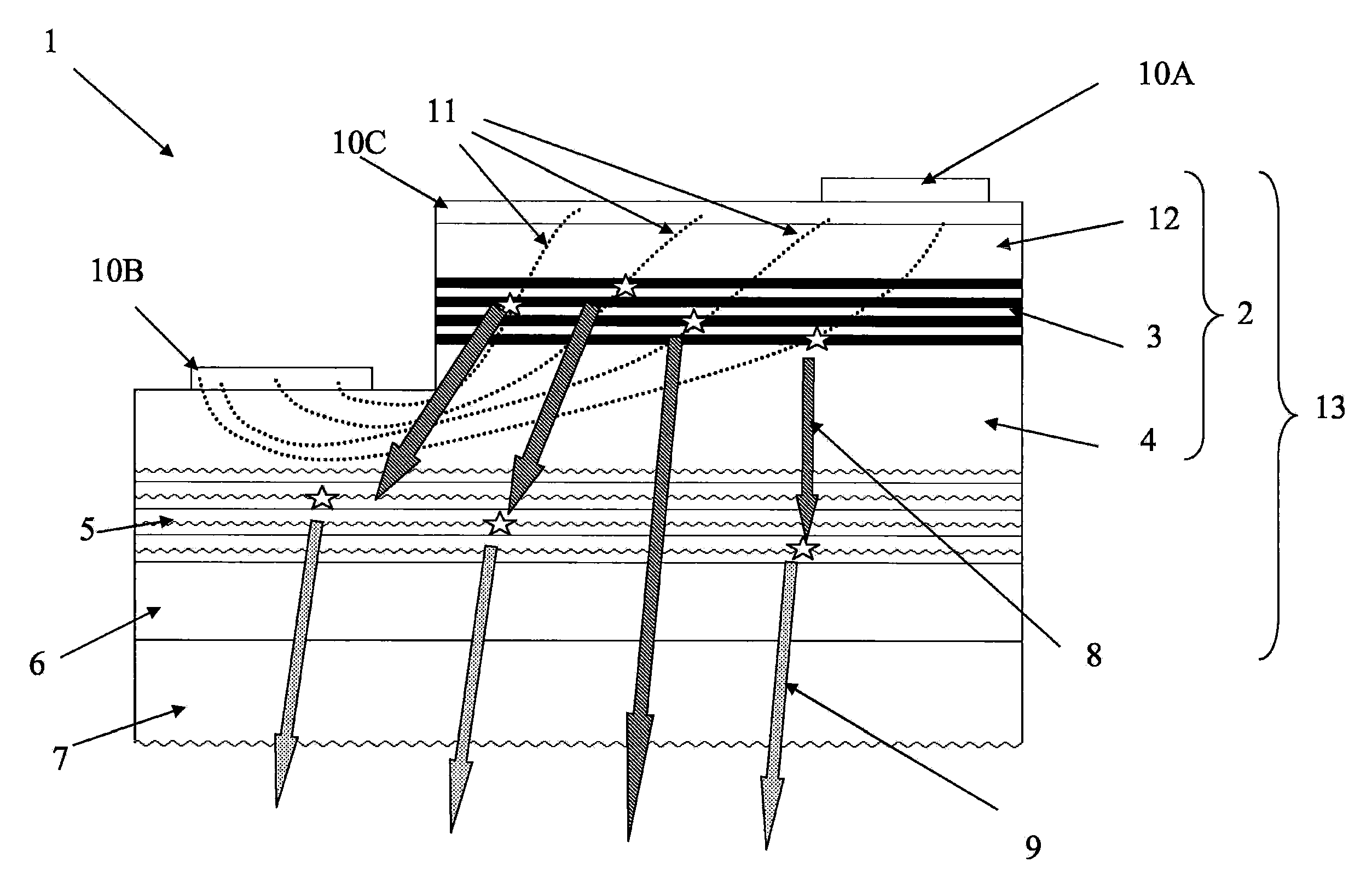
[0026]As illustrated in FIG. 1, a light-emitting diode 1 according to the invention includes a substrate 7 on which a matrix 13 is formed which comprises various portions which will be described in further details hereinunder. The matrix 13 first includes an active portion conducting electric current and more particularly current lines 11. Such electric current is generated by current generating means, for example, by metal contacts in the form of a positive terminal 10A and a negative terminal 10B and a semitransparent contact 10C. The active portion of the matrix 13 is thus defined as the portion of the matrix through which the current emitted by the current generating means 10A, 10B and 10C passes. Such active portion comprises a first zone 3 positioned in the active portion so as to be gone through by the current lines 11. Such zone 3 corresponds to a quantum confinement able to be electrically pumped by the current emitted by the current generating means 10A, 10B and 10C. It wi...


PUM


Abstract

The disclosure relates to a making a matrix of III-V nitride, the matrix including at least an active first portion through which an electrical current passes and at least a passive second portion through which no electrical current passes, the matrix including at least a first zone forming a first quantum confinement region made of a III-V nitride, the first zone being positioned in the active first portion, and at least a second zone forming a second quantum confinement region made of III-V nitride, such that the second zone is positioned to the passive portion of the matrix.

Description

CROSS-REFERENCE TO RELATED APPLICATIONS[0001]This is a divisional of U.S. Ser. No. 12 / 225,039, filed on Sep. 12, 2008, which is a National Phase Entry of International Application Serial No. PCT / FR2007 / 050898, filed on Mar. 9, 2007, which claims priority to French Application Serial No. 06 / 50842, filed Mar. 13, 2006; all of which are incorporated by reference herein.BACKGROUND AND SUMMARY[0002]The present invention relates to the field of light-emitting diodes, and more particularly the field of monolithic light-emitting diodes.[0003]Such diodes are, for example, known from the application U.S. Pat. No. 6,445,009, wherein a diode is disclosed, which comprises a device including a substrate whereon a matrix is positioned, which comprises at least a stack of quantum wells of the GaN or GaInN type emitting in the visible spectrum at an ambient temperature in a layer of AlN or GaN respectively. In the application U.S. Pat. No. 6,445,009, a system of (Al, Ga, In)N or III-V nitrides mater...

Claims


Application Information

Patent Timeline
Patent Type & Authority Applications(United States)
IPC IPC(8): H01L33/40H01L33/08H01L33/50
CPCH01L33/08H01L27/15
Inventor MASSIES, JEANDAMILANO, BENJAMIN
Owner CENT NAT DE LA RECHERCHE SCI
Why Eureka
Try Eureka