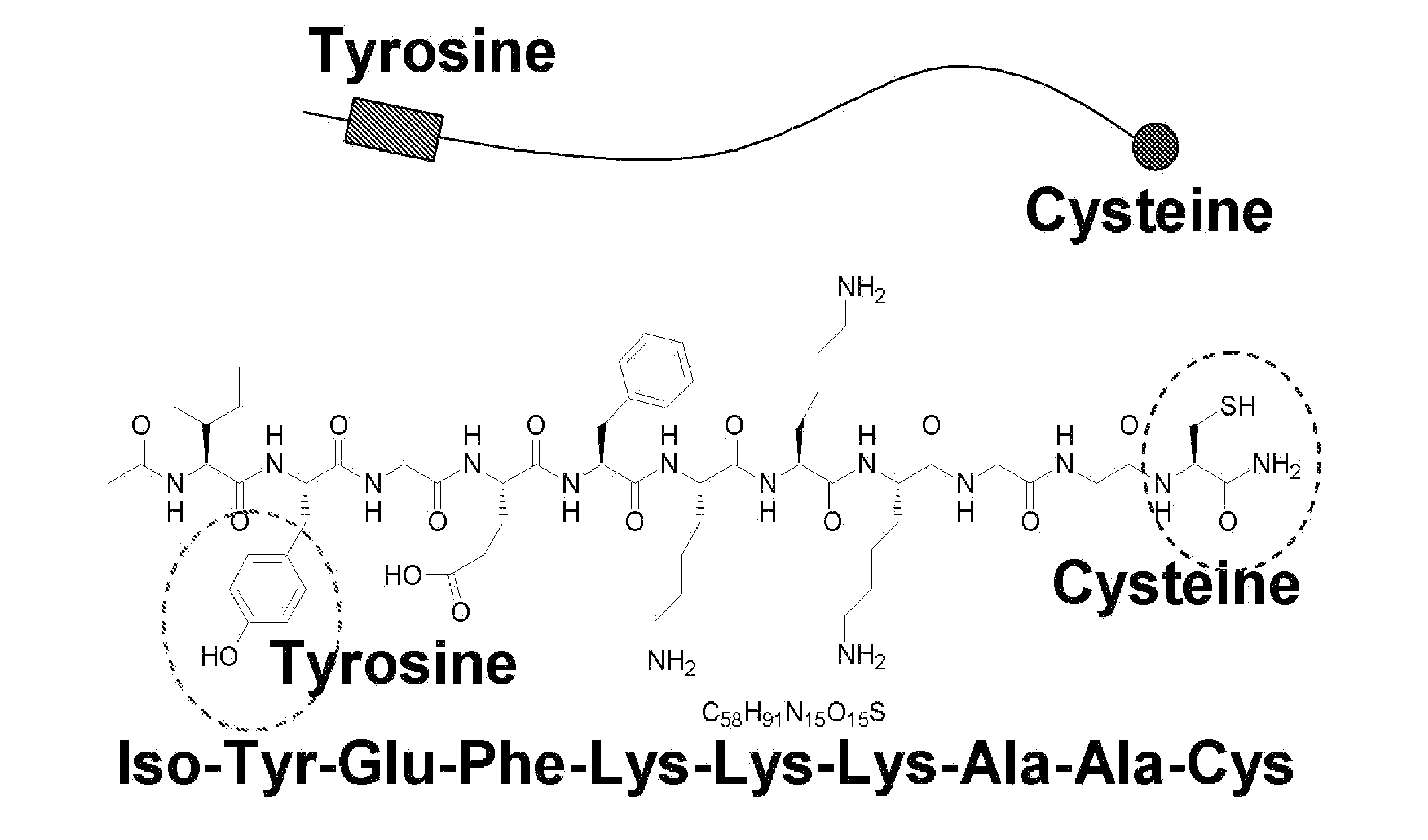
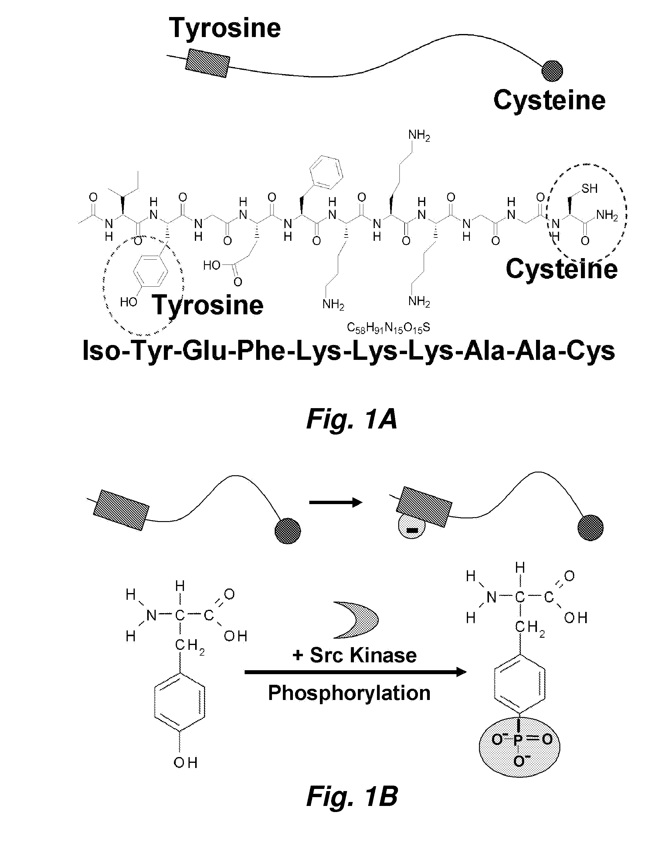
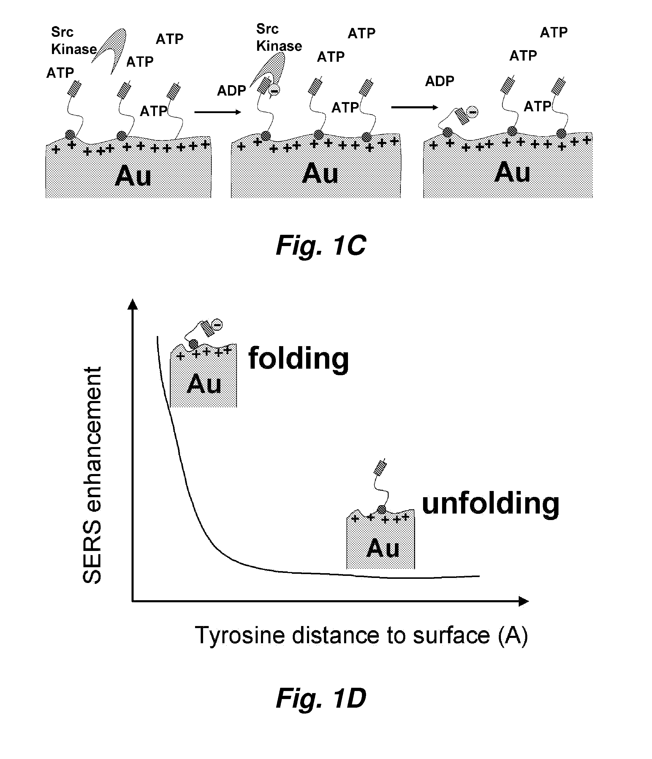
Sers-based, single step, real-time detection of protein kinase and/or phosphatase activity
- Summary
- Abstract
- Description
- Claims
- Application Information
AI Technical Summary
Benefits of technology
Problems solved by technology
Method used
Image

Examples
example 1
Fabrication and Use of SERs Microarray
[0094]Fabrication of Nano Pyramid SERS Substrate
[0095]Starting with a single crystal silicon wafer, a 300 nm thick thin layer of poly-crystal silicon was deposited on the polished top surface of the silicon wafer. Microscale devices can be patterned on the poly-silicon surface using photolithography. After patterning the silicon wafer was etched in a plasma assisted reactive ion etcher. The etching process to make the nano pyramid SERS substrate was different from those used in conventional silicon film etching. At first, the native oxide layer on the poly silicon film was stripped off by using SF6 plasma etching for 10 seconds. Next, a mixture of O2 and HBr gases was flowed in the RF plasma etching chamber for 7 seconds to define nanoscale oxide islands on the top of poly silicon film surface. These nanoscale oxide islands were created by the simultaneous etching and oxidation process. The average diameter of the oxide islands was about 20 nm a...
PUM
 Abstract
Description
Claims
Application Information
 - Generate Ideas
- Intellectual Property
- Life Sciences
- Materials
- Tech Scout
- Unparalleled Data Quality
- Higher Quality Content
- 60% Fewer Hallucinations
Browse by: Latest US Patents, China's latest patents, Technical Efficacy Thesaurus, Application Domain, Technology Topic, Popular Technical Reports.
© 2025 PatSnap. All rights reserved.Legal|Privacy policy|Modern Slavery Act Transparency Statement|Sitemap|About US| Contact US: help@patsnap.com