Impact ionization field-effect transistor

a field-effect transistor and impact ionization technology, applied in the direction of basic electric elements, electrical equipment, semiconductor devices, etc., can solve the problems of reducing affecting the device characteristics, and affecting the performance of conventional field-effect transistors

Active Publication Date: 2011-03-03
GLOBALFOUNDRIES US INC
View PDF7 Cites 20 Cited by
  • Summary
  • Abstract
  • Description
  • Claims
  • Application Information

AI Technical Summary

Problems solved by technology

In this setup, the depletion region lacks sufficient mobile charge carriers to enable carrier flow between source and drain.
One of the main obstacles for improving the performance of conventional field-effect transistors is the fundamental room-temperature (RT) limit of the inverse sub-threshold slope of about 60 mV / decade set by the Fermi distribution function.
This effect is called hot carrier injection into the gate oxide which leads to a hot carrier degradation of the gate oxide after a few voltage sweeps, in turn leading to a degradation of the device characteristics.
The presence of significant hot carrier effects, in particular the injection of charge carriers into the gate dielectric leads to a shift of the threshold voltage and a degradation of the inverse sub-threshold slope over time.
In high performance logic applications such effects are not desired.

Method used


Image

  • Impact ionization field-effect transistor
  • Impact ionization field-effect transistor
  • Impact ionization field-effect transistor

Examples


Embodiment Construction

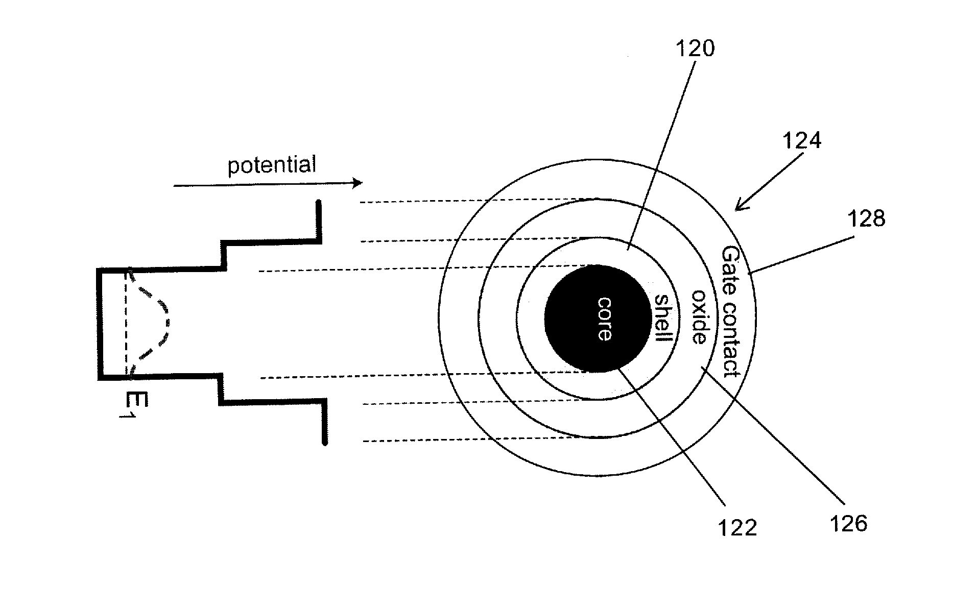
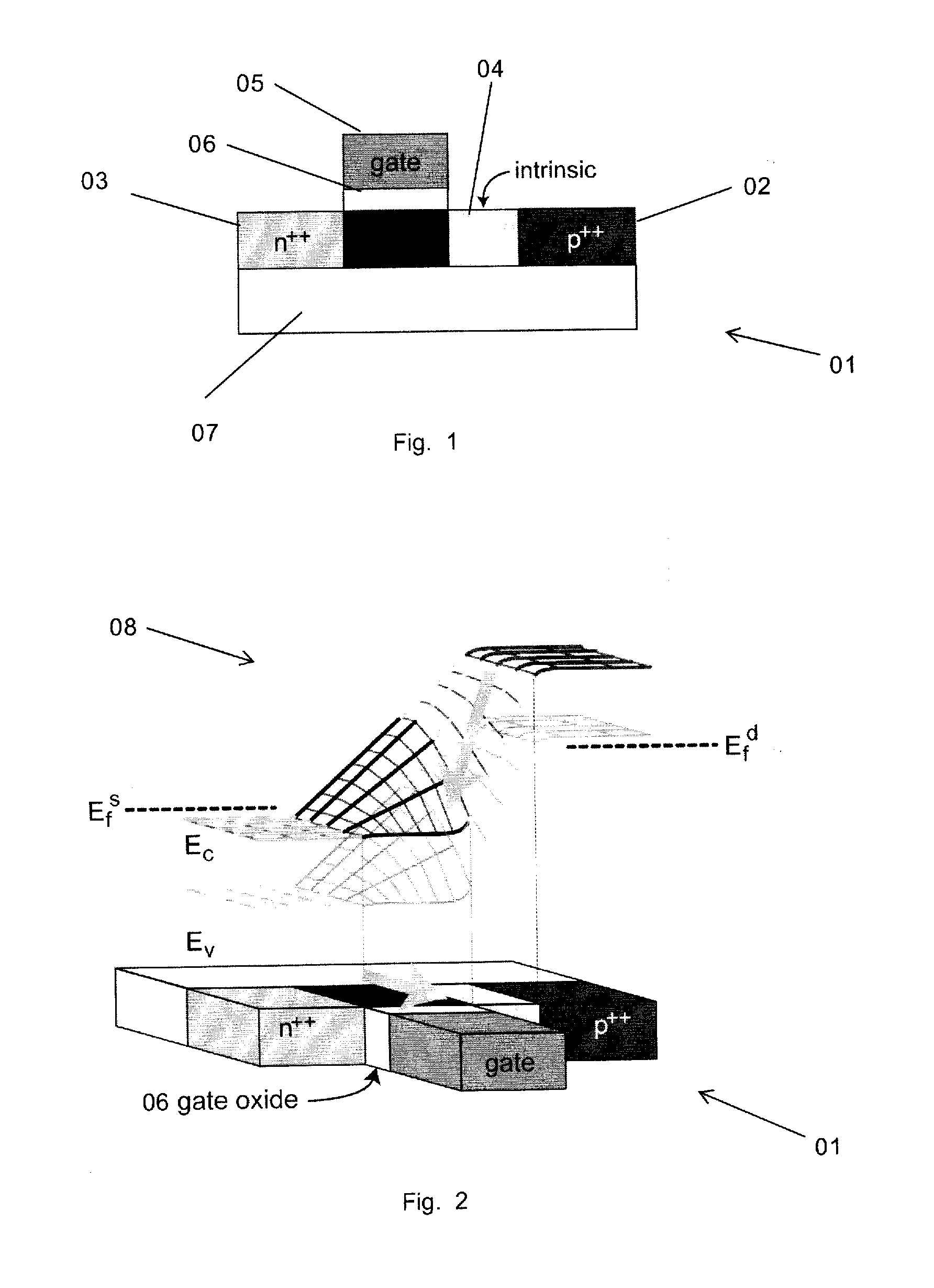
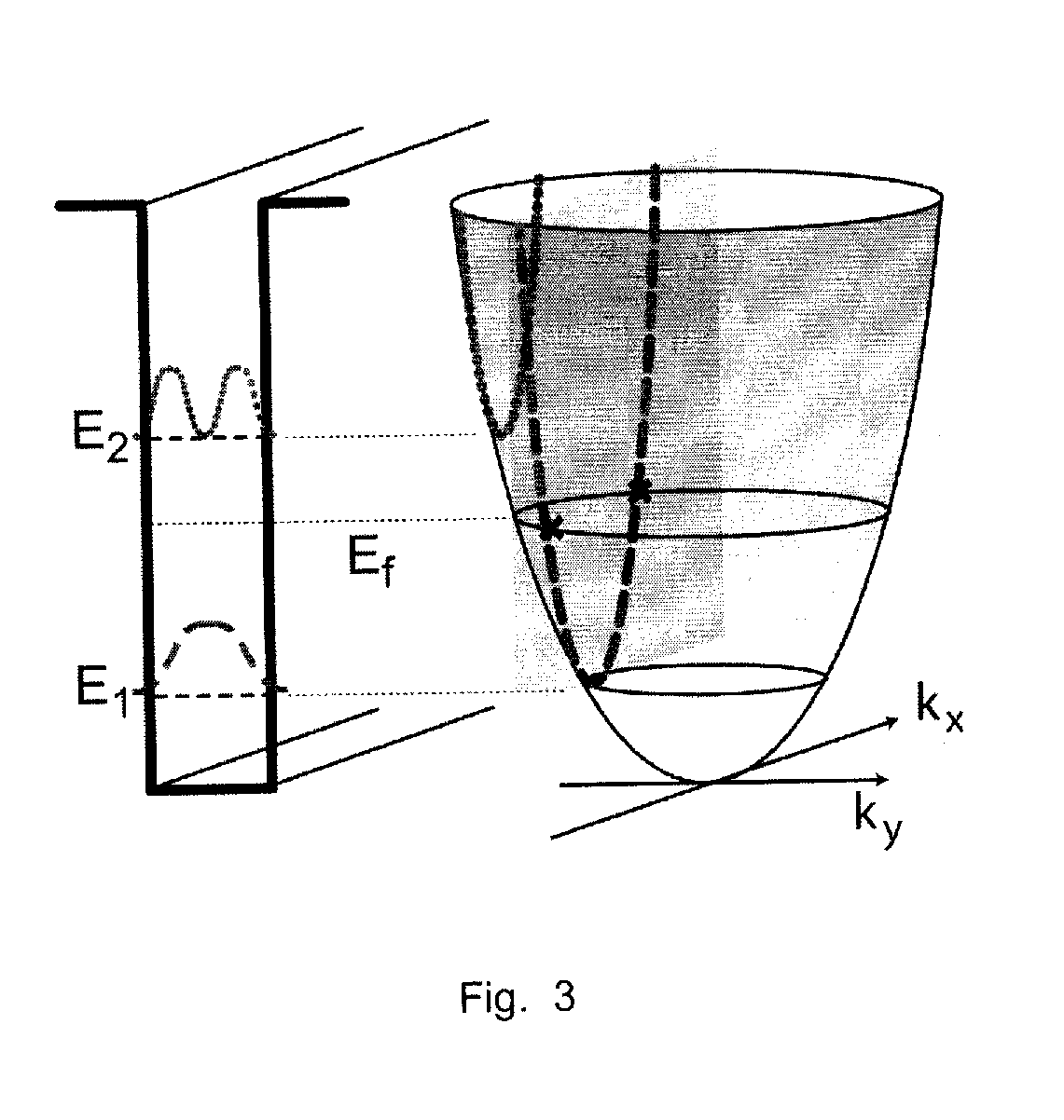
[0025]The principle idea of the invention is that by utilizing quantum confinement effects there is achieved a one-dimensional or at least two-dimensional (in case there is no lateral confinement of the channel) charge carrier transport avoiding (hot) charge carrier acceleration normal to the charge carrier transport, i.e. towards the gate oxide and hence suppressing hot carrier degradation.

[0026]This effect is engineered by providing the channel with a dimension normal to the charge carrier transport for which dimension the energy separation of the first two energy sub-bands of the channel material equals or exceeds the effective energy band gap of the channel material. As a result, a distinct energy sub-band and an appropriate band gap are engineered. This ensures that the charge carriers remain in the first sub-band when reaching the threshold energy for impact ionization. As a result, the charge carrier transport remains one-dimensional in the channel or at least two-dimensional...


PUM


Abstract

An Impact Ionization Field-Effect Transistor (I-MOS) device in which device degradation caused by hot carrier injection into a gate oxide is prevented. The device includes source, drain, and gate contacts, and a channel between the source and the drain. The channel has a dimension normal to the direction of a charge carrier transport in the channel such that the energy separation of the first two sub-bands equals or exceeds the effective energy band gap of the channel material.

Description

CROSS-REFERENCE TO RELATED APPLICATION[0001]This application claims priority under 35 U.S.C. 119 from European Application 09169056.0 filed Aug. 31, 2009, the entire contents of which are incorporated herein by reference.BACKGROUND OF THE INVENTION[0002]1. Field of the Invention[0003]The invention relates to an impact ionization field-effect transistor (I-MOS or I-MOSFET). More particularly, the invention relates to an I-MOS in which device degradation caused by hot carrier injection into a gate oxide is prevented.[0004]2. Description of Related Art[0005]Field-effect transistors typically include source, drain, and gate contacts and / or terminals. The characteristics of a channel region between the source and drain are controlled by applying a voltage to the gate contact in which the gate is separated from the channel by an insulating layer such as an oxide layer. Source, drain and channel typically include a semiconductor material. Subject to the set-up of the field-effect transisto...

Claims


Application Information

Patent Timeline
Patent Type & Authority Applications(United States)
IPC IPC(8): H01L29/775
CPCH01L29/7391H01L29/0665
Inventor BJOERK, MIKAEL T.HAYDEN, OLIVERKNOCH, JOACHIMLOERTSCHER, EMANUELRIEL, HEIKE E.RIESS, WALTER HEINRICHSCHMID, HEINZ
Owner GLOBALFOUNDRIES US INC
Why Eureka
Try Eureka