Semiconductor integrated circuit

a technology of integrated circuits and semiconductors, applied in the direction of logic circuits, semiconductor devices, pulse techniques, etc., can solve the problems of inconvenient single-height configuration, inability to secure a space to connect the gates together with the upper layer wirings, and several gate lines that must be further shorted together, so as to reduce the number of internal wirings, eliminate waste of space, and increase the standard cell length of multi-height cells

Active Publication Date: 2011-03-03
SONY CORP
View PDF1 Cites 74 Cited by
  • Summary
  • Abstract
  • Description
  • Claims
  • Application Information

AI Technical Summary

Benefits of technology

[0019]In the above configuration of the semiconductor integrated circuit according to the embodiment of the present invention, if electrical shorting is required for in-phase driving, the gate electrodes of a plurality of complementary transistor pairs to be driven in phase are formed integrally with a common gate line itself. This provides a reduced number of internal wirings required to short the gate lines, thus eliminating wasted space. Further, this eliminates the need to form internal wirings in complex shapes.
[0020]The above preferable configuration does not impede the advantages of the standard cell layout system because the multi-height cells preferably have a power line sharing structure with the adjacent single height cells. At this time, the single height cells need only have a required minimum basic cell length suitable for a small-scale circuit. The standard cell length of the multi-height cell is a plurality of times the basic cell length thereof. This makes it possible to secure a power line sharing structure with other surrounding cells even if the standard cell length of the multi-height cell is increased. Further, in this case, the single height cell has a required minimum basic cell length suitable for a small-scale circuit, thus eliminating wasted space.
[0021]The present invention provides a semiconductor integrated circuit having a cell layout unlikely to produce wasted space and advantageous in terms of cost when the semiconductor integrated circuit contains standard cells for achieving a circuit adapted to drive a plurality of complementary transistor pairs (e.g., CMOS pairs) in phase.

Problems solved by technology

However, there are cases in which the single height configuration is not suitable depending on the circuit scale.
However, several gate lines must be further shorted together.
As a result, it may be impossible to secure a space to connect the gates together with the upper layer wirings.
Even if a space is secured, it may be necessary to design wirings that are bent in a complex manner, thus resulting in reduced workability for design and mask preparation and leading to higher cost.

Method used


Image

  • Semiconductor integrated circuit
  • Semiconductor integrated circuit
  • Semiconductor integrated circuit

Examples


first embodiment

1. First Embodiment

1. Overall Layout

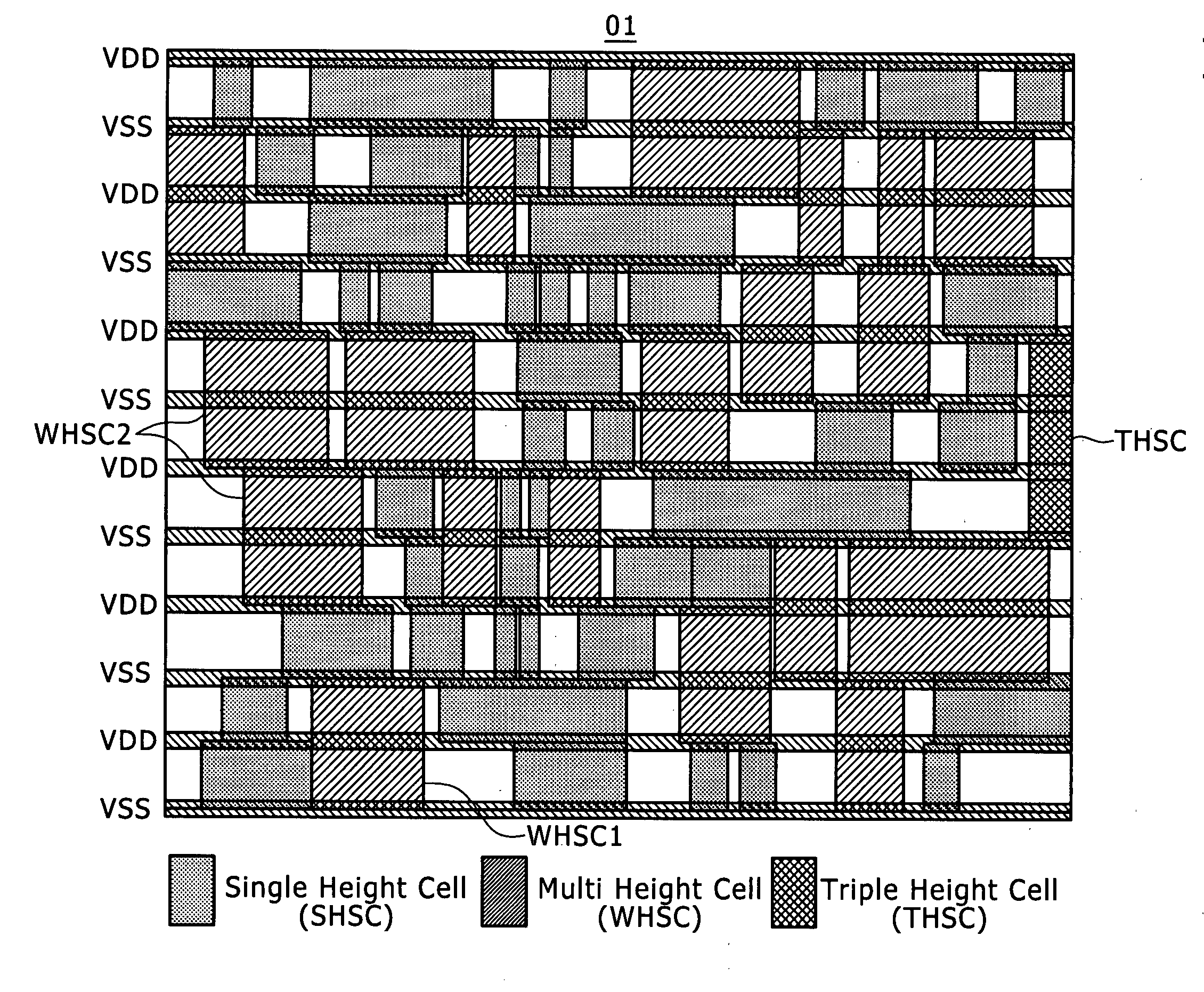
[0040]FIG. 1 is a diagram schematically illustrating a plan view of an integrated circuit according to embodiments with a focus on the cell layout.

[0041]In FIG. 1, each of rectangular areas is called a cell. The cells denoted by reference numeral SC are standard cells. The standard cell SC is a predesigned and standardized functional circuit cell registered in a library such as an inverter or a NAND gate. Although being a collection of data, the standard cell SC may refer to part of a device manufactured based on the data. Although a detailed description will be given later, standard cells registered in a library are combined and laid out in the design phase of a semiconductor integrated circuit. As a result of the layout, source voltage lines and reference voltage lines (e.g., GND lines) are roughly connected together on data. Connecting signal and other lines after the layout provides the desired circuit. The layout of cells and disposition of w...

first application example

[0063]FIG. 3 is an equivalent circuit diagram of a half adder cell as a circuit example of the standard cell SC to which the present invention is applied. The half adder shown in FIG. 3 is broadly divided into a carry-out section (CO section) and a single-bit addition section (Sum section). The half adder is a circuit designed to receive first and second input bits (A1 and A2) and output a half addition bit (S) and a carry-out bit (hereinafter the CO bit). The half addition bit represents the result of half addition in the first digit. The CO bit represents a carry.

[0064]It should be noted that the gates of the CMOS pairs that are supplied, for example, with the same input in FIG. 3 are indicated by bi-directional arrows.

[0065]The carry-out (CO) section includes a NAND circuit and an inverter. The NAND circuit includes two PMOS transistors P1 and P2 and two NMOS transistors N1 and N2. The inverter includes a PMOS transistor P3 and an NMOS transistor N3. The NAND circuit and inverter...

second application example

[0107]FIGS. 6A and 6B illustrate a circuit symbol and equivalent circuit diagram of a clock buffer cell.

[0108]A clock buffer cell is a cell including an even number of stages of cascaded inverters. This type of cell is designed so that the clock output from the cell has the same duty ratio to the extent possible. Therefore, a clock buffer is characterized in including larger-than-normal PMOS transistors or smaller-than-normal NMOS transistors.

[0109]A specific clock buffer circuit includes two cascaded inverters INV1 and INV2 shown in FIG. 6A. Each of the inverters INV1 and INV2 includes two inverters connected in parallel as shown in FIG. 6B. Thus, when each of the inverters INV1 and INV2 of the clock buffer at the first and second stages includes two inverters connected in parallel, the inverters offer sufficient driving capability. In addition, the present invention is more readily applicable to the clock buffer.

[0110]FIG. 7 illustrates an example in which the circuit shown in FIG...


PUM


Abstract

Disclosed herein is a semiconductor integrated circuit, wherein a desired circuit is formed by combining and laying out a plurality of standard cells and connecting the cells together, of which the cell length, i.e., the gap between a pair of opposed sides, is standardized, the plurality of standard cells forming the desired circuit include complementary in-phase driven standard cells, each of which includes a plurality of complementary transistor pairs that are complementary in conductivity type to each other and have their gate electrodes connected together, and N (≧2) pairs of all the complementary transistor pairs are driven in phase, and the size of the standardized cell length of the complementary in-phase driven standard cell is defined as an M-fold cell length which is M (N≧M≧2) times the basic cell length which is appropriate to the single complementary transistor pair.

Description

BACKGROUND OF THE INVENTION[0001]1. Field of the Invention[0002]The present invention relates to a semiconductor integrated circuit having a desired circuit formed by combining and laying out a plurality of standard cells each having transistors and gate electrodes and connecting the cells together.[0003]2. Description of the Related Art[0004]In a common standard cell, at least one of the sizes thereof in the directions orthogonal to each other (so-called vertical and horizontal directions) is standardized to a few types or, for example, to three types. The so-called vertical size is referred to as the height of the standard cell. This height is standardized to three types or so. Here, in order to avoid confusion between this cell size (height) and its structural height perpendicular to the semiconductor substrate, the cell size will not be called the “height.” Instead, this size will be referred to as the “standard cell length” for the sake of convenience.[0005]Even when a few stan...

Claims


Application Information

Patent Timeline
Patent Type & Authority Applications(United States)
IPC IPC(8): H01L27/06
CPCH01L27/11807H01L27/0207
Inventor TANAKA, YOSHINORI
Owner SONY CORP
Why Eureka
Try Eureka