Patch antenna with wide bandwidth at millimeter wave band

a technology of patch antenna and millimeter wave band, which is applied in the direction of antenna earthing, substantially flat resonant elements, resonant antennas, etc., can solve the problems of reducing the radiation efficiency and gain of patch antenna, difficult to achieve the desired wideband characteristics, and difficult to meet such requirements by using a typical patch antenna structure. achieve the effect of wideband characteristics, suppressing signal leakage, and reducing the size and manufacturing costs of modules

Inactive Publication Date: 2011-03-10
ELECTRONICS & TELECOMM RES INST
View PDF5 Cites 127 Cited by
  • Summary
  • Abstract
  • Description
  • Claims
  • Application Information

AI Technical Summary

Benefits of technology

[0007]The present invention provides a patch antenna configured to suppress signal leakage in the form of surface waves along the surface of a dielectric substrate, provide wideband characteristics, and reduce the size and manufacturing costs of modules.
[0011]In other embodiments, the vias may function as a metal wall suppressing leakage of a signal accumulated in the center region.

Problems solved by technology

Such signal leakage decreases the radiation efficiency and gain of the patch antenna.
Although 60-GHz band communication systems require a wide bandwidth of 7 GHz or wider, it is difficult to satisfy such requirement by using a typical patch antenna structure.
However, a ceramic substrate such as an LTCC substrate has higher dielectric constant than an organic substrate, and thus, if the ceramic substrate is used to form the patch antenna, since the radiation efficiency and gain of the patch antenna are low as described above, the number of antenna arrays should be much increased to obtain desired antenna gain, and it is difficult to obtain desired wideband characteristics.
Thus, the size and manufacturing costs of modules are increased as compared with the case where the entire system including the antenna patch is mounted on an LTCC substrate in the form of an SOP.

Method used


Image

  • Patch antenna with wide bandwidth at millimeter wave band
  • Patch antenna with wide bandwidth at millimeter wave band
  • Patch antenna with wide bandwidth at millimeter wave band

Examples


first embodiment

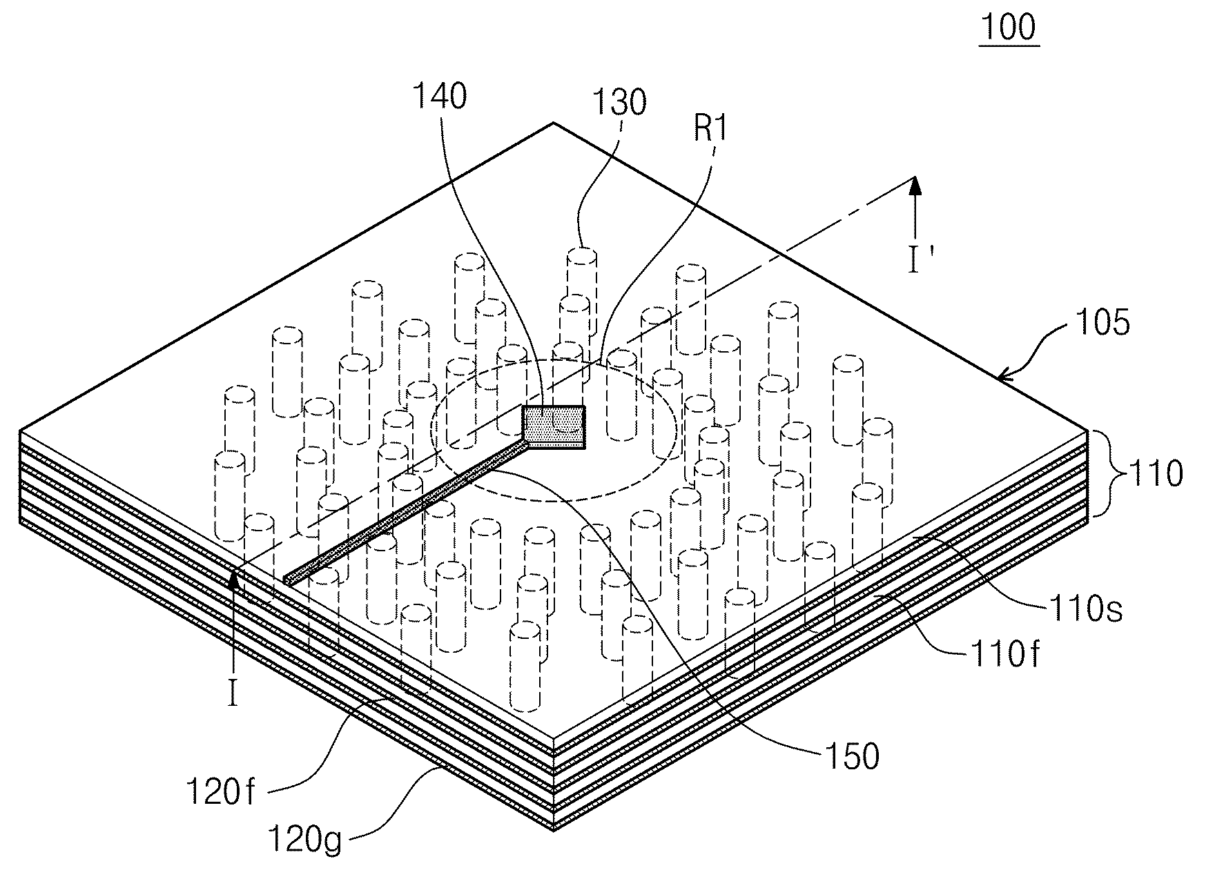
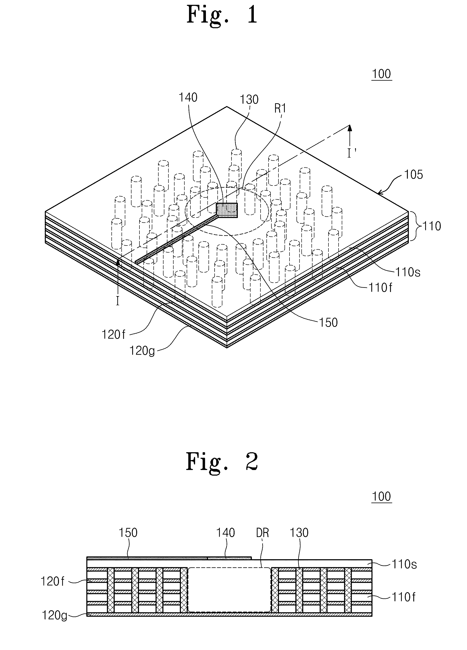
[0042]FIG. 1 is a perspective view illustrating a millimeter wave band patch antenna according to the present invention, and FIG. 2 is a sectional view taken along line I-I′ of FIG. 1.

[0043]Referring to FIGS. 1 and 2, a patch antenna 100 includes: a multi-layer substrate 105 in which a plurality of dielectric layers 110f and 110s (inner dielectric layers 110f and a surface dielectric layer 110s) are stacked; metal pattern layers 120f disposed between the dielectric layers 110f and 110s except for an center region R1 of the multi-layer substrate 105; an antenna patch 140 disposed on an upper surface of the multi-layer substrate 105 in the center region R1; a ground layer 120g disposed on a lower surface of the multi-layer substrate 105 opposing to the upper surface of the multi-layer substrate 105; and a plurality of vias 130 formed through the inner dielectric layers 110f around the center region R1 so as to connect the metal pattern layers 120f to the ground layer 120g. The center ...

second embodiment

[0072]FIG. 7 is a perspective view illustrating a millimeter wave band patch antenna according to the present invention.

[0073]Referring to FIG. 7, a patch antenna 200 of the current embodiment has metal pattern layers 220f different from the metal pattern layers 120f of the first embodiment illustrated in FIG. 1. The metal pattern layers 220f may be a plurality of line patterns extending radially from a center region R1 of a multi-layer substrate 205.

[0074]As described above in FIGS. 1 and 2, a plurality of vias 230 surrounding the center region R1 of the multi-layer substrate 205 are spaced from each other by about half (λ / 2) the wavelength of radiation of an antenna patch 240, and thus radiation (having a wavelength λ) of the antenna patch 240 cannot propagate between the vias 230. That is, by using only the vias 230 surrounding the center region R1 of the multi-layer substrate 205, signal leakage from the antenna patch 240 in the form of surface waves can be directed to a dielect...


PUM


Abstract

Provided is a millimeter wave band patch antenna. The patch antenna includes a multi-layer substrate, at least one metal pattern layer, an antenna patch, a ground layer, and a plurality of vias. In the multi-layer substrate, a plurality of dielectric layers are stacked. The metal pattern layer is disposed between the dielectric layers except for a center region of the multi-layer substrate. The antenna patch is disposed on an upper surface of the multi-layer substrate in the center region. The ground layer is disposed on a lower surface of the multi-layer substrate opposing to the upper surface. The vias is disposed around the center region through the dielectric layers for electrically connecting the metal pattern layer to the ground layer. The center region, which is surrounded by the ground layer and the vias, functions as a resonator.

Description

CROSS-REFERENCE TO RELATED APPLICATIONS[0001]This U.S. non-provisional patent application claims priority under 35 U.S.C. §119 of Korean Patent Application No. 10-2009-0084400, filed on Sep. 8, 2009, the entire contents of which are hereby incorporated by reference.BACKGROUND OF THE INVENTION[0002]The present invention disclosed herein relates to a patch antenna with wide bandwidth at millimeter wave band, and more particularly, to a high-gain, high-efficiency, wideband millimeter wave band patch antenna constructed on a multi-layer substrate.[0003]Frequencies of the millimeter wave band are more straightforward and have wideband characteristics as compared with those of micro wave band, thereby drawing attention in application to radars and communication services. Particularly, since wavelengths of the millimeter wave band are short, it is easy to manufacture small antennas and thus reduce system sizes largely. Among communication services in the millimeter wave band, 60-GHz broadb...

Claims


Application Information

Patent Timeline
Patent Type & Authority Applications(United States)
IPC IPC(8): H01Q1/38H01Q1/48
CPCH01Q1/48H01Q9/0442H01Q9/0407H01Q1/38H01Q13/08H01Q9/04
Inventor KIM, DONG-YOUNGKIM, HAE CHEON
Owner ELECTRONICS & TELECOMM RES INST
Why Eureka
Try Eureka