Semiconductor device and method for manufacturing the same

a technology of semiconductor devices and semiconductors, applied in the direction of semiconductor devices, basic electric elements, electrical equipment, etc., can solve the problems of air gap space on the substrate surface, increase in processing time and cost, and long flow time, and achieve the effect of high fillability

Active Publication Date: 2011-03-17
RENESAS ELECTRONICS CORP
View PDF5 Cites 61 Cited by
  • Summary
  • Abstract
  • Description
  • Claims
  • Application Information

AI Technical Summary

Benefits of technology

[0008]The present invention has been made in view of the above problem and has an object to provide a semiconductor device which eliminates the need for high fillability through a simple process and a method for manufacturing the same.
[0010]According to this aspect of the invention, the first trench is made after completion of the device, so there is no possibility that photo-resist may get into the first trench in the course of making the device. Therefore, a semiconductor device which eliminates the need for high fillability through a simple process and a method for manufacturing the same can be realized.

Problems solved by technology

This means that an insulating film deposition process must be performed twice and an anisotropic etching process to expand the upper end of the opening must also be performed, resulting in a longer flow time and an increase in processing time and cost.
In addition, if there is an air-gap space in the trench, the air-gap space may become exposed on the substrate surface by a subsequent wet process.
If the air-gap space in the trench is exposed on the substrate surface, photo-resist may get into the air-gap space through its exposed portion and become unremovable.
The photo-resist in the air-gap space may spout and appear as a foreign substance in a later process, causing a pattern defect.

Method used


Image

  • Semiconductor device and method for manufacturing the same
  • Semiconductor device and method for manufacturing the same
  • Semiconductor device and method for manufacturing the same

Examples


first embodiment

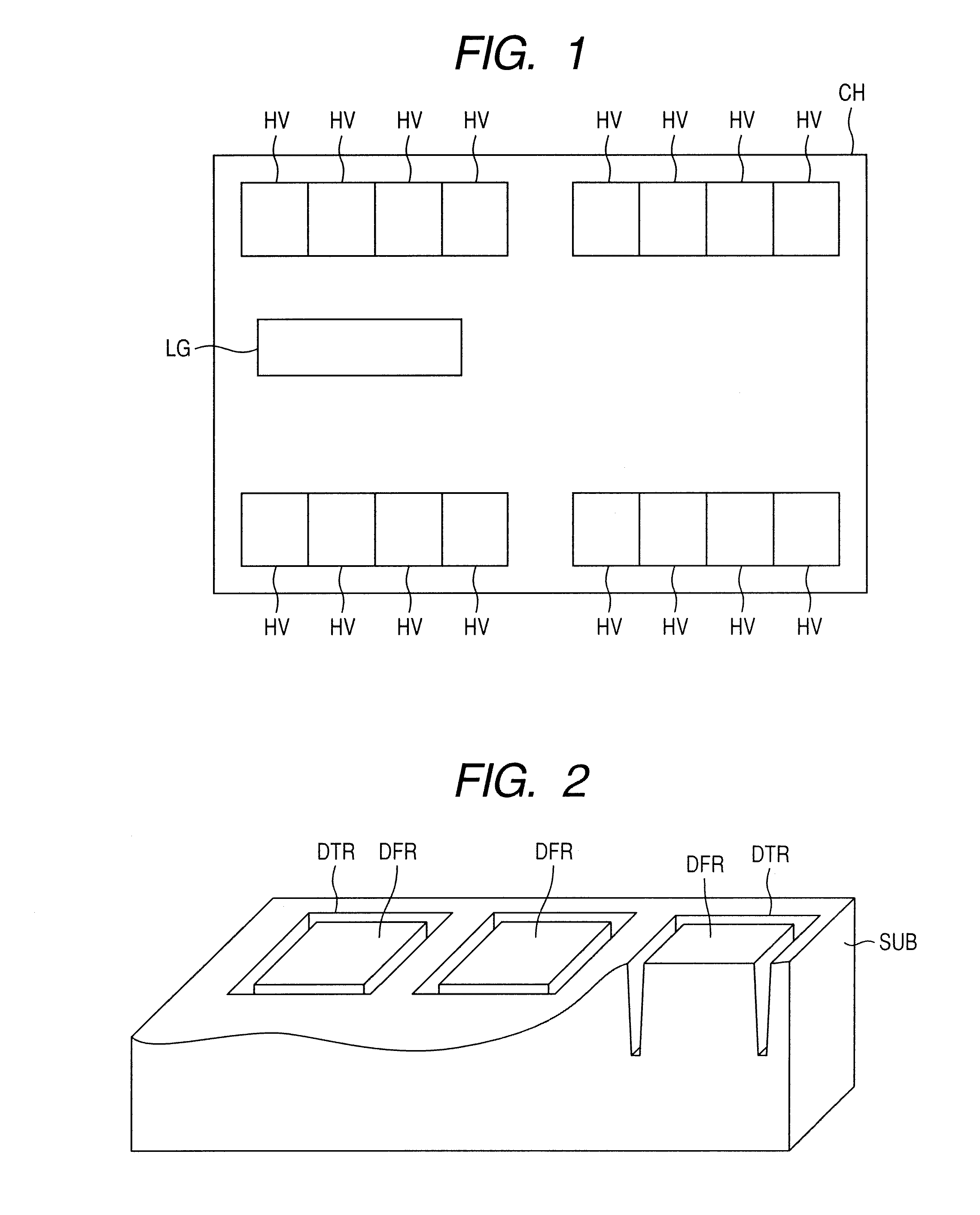
[0042]Referring to FIG. 1, a BiC-DMOS (bipolar complementary double-diffused metal oxide semiconductor) chip CH has a logic section LG, for example, as an integration of low breakdown voltage CMOS (complementary MOS) transistors, and output drivers HV which use high breakdown voltage devices. The region in which the logic section LG is formed is surrounded by a DTI structure when seen in a plan view. In the output drivers HV, each device formation region is surrounded by a DTI structure when seen in a plan view.

[0043]Referring to FIG. 2, in the output drivers HV, the device formation region DFR for each high breakdown voltage device is surrounded by a trench DTR configuring a DTI structure when seen in a plan view. This trench DTR is formed in a surface of a semiconductor substrate SUB.

[0044]Next, a case that a high breakdown voltage lateral MOS transistor is used as the high breakdown voltage device will be explained.

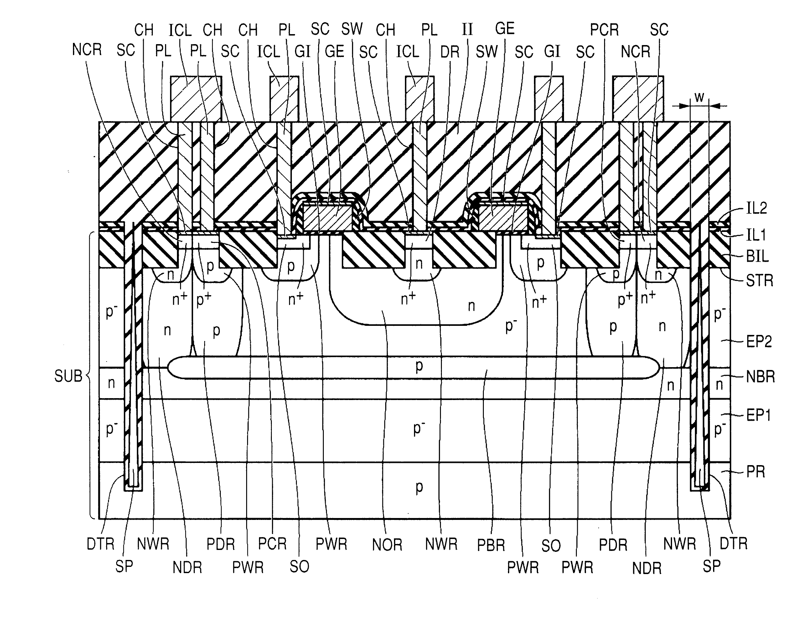
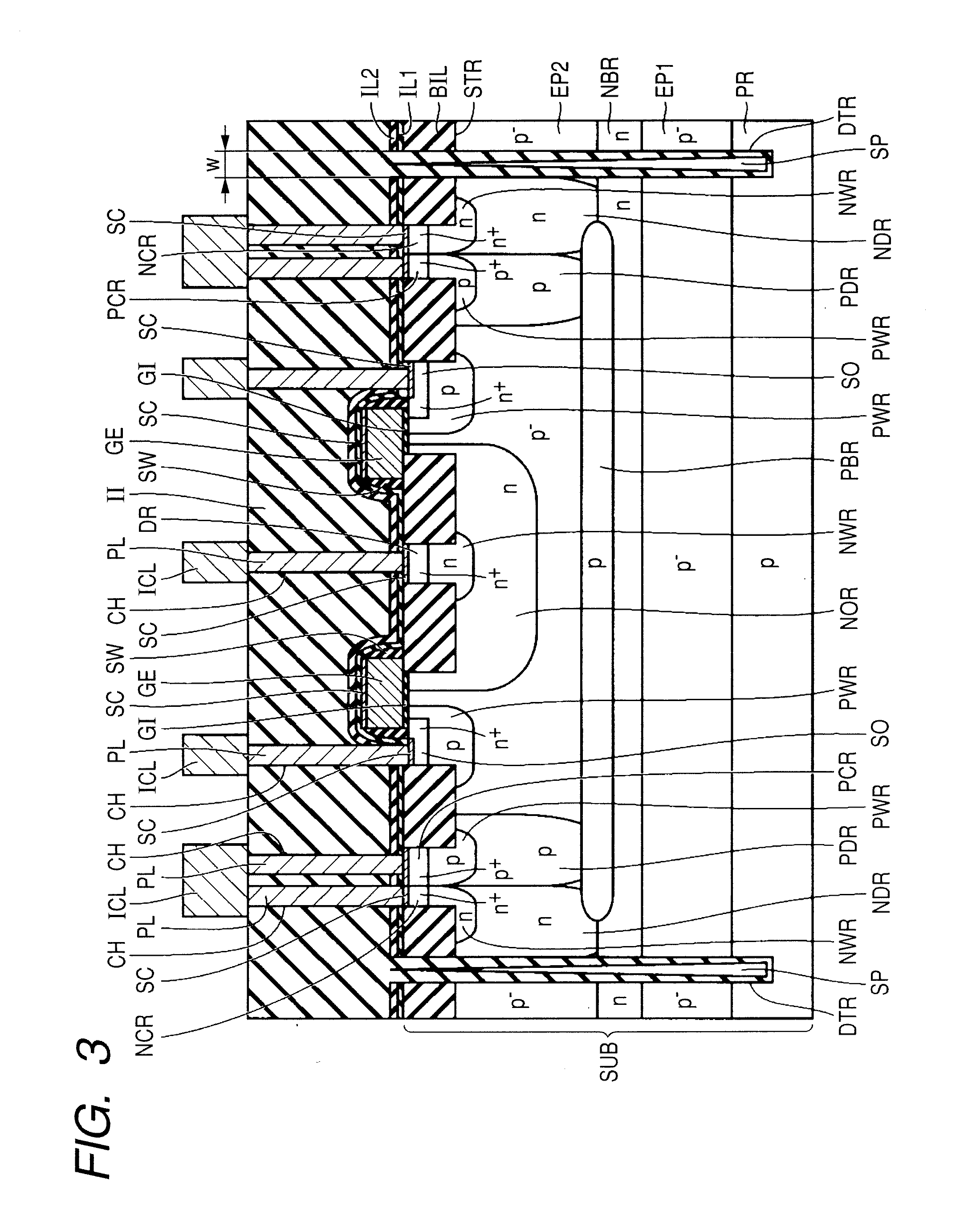
[0045]Referring to FIG. 3, the semiconductor substrate SUB is, fo...

second embodiment

[0092]Although the first embodiment concerns a DTI structure which is formed in a region where an STI structure exists, a DTI structure may be formed in a region where no STI structure exists. The second embodiment, in which a DTI structure is formed in a region where no STI structure exists, is described below.

[0093]Referring to FIG. 18, an insulating film IL1, an insulating film IL2 and a mask film MK are stacked over the surface of a semiconductor substrate SUB in order. This process corresponds to the steps before photo-resist PRE coating in the first embodiment as shown in FIG. 5.

[0094]Referring to FIG. 19, anisotropic etching is performed on the mask film MK, insulting film IL2 and insulating film IL1 in order by an ordinary photoengraving technique and an etching technique.

[0095]Then, anisotropic etching is performed on the semiconductor substrate SUB using the patterned mask film MK as a mask. Consequently, a trench DTR extending inward from the surface of the semiconductor ...

third embodiment

[0099]Although the mask film MK is removed by isotropic etching in the manufacturing process according to the second embodiment, the mask film MK need not necessarily be removed. The third embodiment, in which the mask film MK is not removed, is described below.

[0100]The manufacturing method according to the third embodiment includes the same steps as shown in FIGS. 18 and 19 in the second embodiment. Referring to FIG. 21, after these steps, insulating film IIA is formed over the mask film MK and in the trench DTR in a manner to cover the device (not shown) and form an air-gap space SP in the trench DTR without removing the mask film MK.

[0101]Then, the same steps as those shown in FIGS. 10 to 12 in the first embodiment are carried out to manufacture a semiconductor device with the mask film MK not removed according to the third embodiment.

[0102]According to the third embodiment, the step of removing the mask film MK is omitted, leading to further cost reduction and shorter turnaroun...


PUM


Abstract

A semiconductor device which eliminates the need for high fillability through a simple process and a method for manufacturing the same. A high breakdown voltage lateral MOS transistor including a source region and a drain region is completed on a surface of a semiconductor substrate. A trench which surrounds the transistor when seen in a plan view is made in the surface of the semiconductor substrate. An insulating film is formed over the transistor and in the trench so as to cover the transistor and form an air-gap space in the trench. Contact holes which reach the source region and drain region of the transistor respectively are made in an interlayer insulating film.

Description

CROSS-REFERENCE TO RELATED APPLICATIONS[0001]The disclosure of Japanese Patent Application No. 2009-213345 filed on Sep. 15, 2009, including the specification, drawings and abstract, is incorporated herein by reference in its entirety.BACKGROUND OF THE INVENTION[0002]The present invention relates to a semiconductor device and a method for manufacturing the same and more particularly to a semiconductor device having a trench and a method for manufacturing the same.[0003]A device isolation (deep trench isolation, or DTI) structure in which insulating film is filled in a trench with a high aspect ratio is disclosed in Japanese Unexamined Patent Publication No. 2002-118256.[0004]In the technique described therein, a trench is first made in a surface of a semiconductor substrate and then a first insulating film is formed over the surface of the semiconductor substrate in a manner to fill the trench. An opening which reaches the first insulating film is made by anisotropic etching of the ...

Claims


Application Information

Patent Timeline
Patent Type & Authority Applications(United States)
IPC IPC(8): H01L29/02H01L21/76
CPCH01L21/764H01L29/0649H01L21/823814H01L21/82385H01L21/823857H01L21/823878H01L21/823892H01L27/0922H01L27/11521H01L27/11526H01L29/0653H01L29/0878H01L29/1083H01L29/1087H01L29/456H01L29/4933H01L29/66689H01L29/7816H01L29/7835H01L21/823807H10B41/30H10B41/40H01L21/8249
Inventor ONISHI, KAZUMAOTSU, YOSHITAKAKIMURA, HIROSHINITTA, TETSUYAYANAGI, SHINICHIROMORII, KATSUMI
Owner RENESAS ELECTRONICS CORP
Why Eureka
Try Eureka