Photospectrometer

a technology of photospectrometer and spectrometer, which is applied in the field of photospectrometry, can solve the problems of increasing the complexity and cost of a photospectrometer

Active Publication Date: 2011-03-17
SOFTKINETIC SENSORS
View PDF8 Cites 7 Cited by
  • Summary
  • Abstract
  • Description
  • Claims
  • Application Information

AI Technical Summary

Benefits of technology

[0005]It is an object of embodiments of the present invention to provide good apparatus or methods for performing photospectrometry, i.e. for retrieving spectral information of a source of electromagnetic radiation, e.g. for identifying an unknown spectrum of a source of electromagnetic radiation.

Problems solved by technology

The above known types of detection techniques involve the use of extra optical components such as filters, or diffractive, refractive, interferometric or dispersive components, which increases the complexity and cost of a photospectrometer.

Method used


Image

  • Photospectrometer
  • Photospectrometer
  • Photospectrometer

Examples


first embodiment

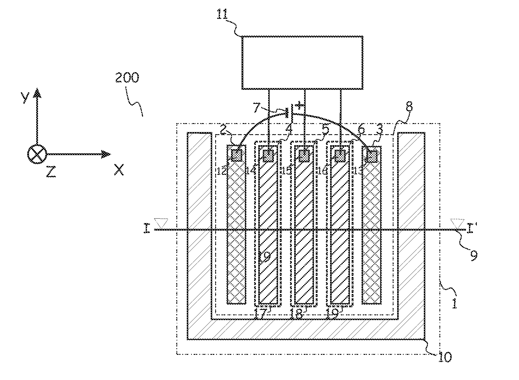
[0056]FIG. 1A shows the top view of a photo-spectrometer 200 according to the present invention. FIG. 1B shows a cross-section according to line I-I′ in FIG. 1A. The photo-spectrometer 200 comprises a resistive, lightly doped semiconductor substrate 1 having a first conductivity type, in the example given a p-type substrate. The lightly doped semiconductor substrate 1 has a doping level ranging from intrinsic (undoped) to a doping level corresponding to a volume resistivity of about 20 Ohm·cm.

[0057]In embodiments of the present invention, the term “substrate” may include any underlying material or materials that may be used, or upon which a spectrometer device may be formed. In embodiments, this “substrate” may include a semiconductor substrate such as e.g. doped silicon, a gallium arsenide (GaAs), a gallium arsenide phosphide (GaAsP), an indium phosphide (InP), a germanium (Ge), or a silicon germanium (SiGe) substrate. The “substrate” may include for example an insulating layer suc...

second embodiment

[0069]FIG. 2A shows a top view of a photospectrometer 202 in accordance with the present invention, whereby impinging electromagnetic radiation, e.g. light, is captured by an electromagnetically sensitive area, e.g. an optically sensitive area 50, which is separate from the detection regions 4, 5 and 6. The number of detection regions illustrated in this embodiment is three; however, this is not limiting for the present invention. More or less detection regions can be present. The detection regions are covered by a radiation shielding, e.g. a shielding metal 10. This way, the sensitive area is surrounded by the radiation shielding.

[0070]FIG. 2B represents a cross-section along the line Y-Y′ of the photo-spectrometer embodiment illustrated in FIG. 2A. Impinging electromagnetic radiation, e.g. light, generates electron hole pairs with a lateral distribution depending in the lateral intensity distribution of the radiation and a vertical distribution depending on the spectrum of the imp...

third embodiment

[0072]FIG. 3A shows a top view of a photospectrometer 204 according to the present invention. In this embodiment, the detection regions, in the example illustrated detections regions 70 to 81, are spread in an array along 2 dimensions of the substrate 1. In the example illustrated the array is a regular array; however, this is not limiting for the present invention. A plurality of conductive regions is provided, for sourcing or draining current from a plurality of current sources. In the example illustrated, four conductive regions 60, 61, 62, 62 are provided, at the corners of the array of detection regions 70 to 81. This, again, is not intended to be limiting for the present invention. A different number of conductive regions, between two and any suitable number higher than two, may be provided. Moreover, these conductive regions do not need to be placed at corners of an array of detection regions. In alternative embodiments, the plurality of conductive regions could be placed aro...


PUM


Abstract

Impinging electromagnetic radiation generates pairs of majority and minority carriers in a substrate. A spectrometer device for detection of electromagnetic radiation impinging on a substrate comprises means for generating, in the substrate, a majority carrier current; at least one detection region for collecting generated minority carriers, the minority carriers being directed under influence of the majority carrier current; and means for determining spectral information based on minority carriers collected at the at least one detection region.

Description

TECHNICAL FIELD OF THE INVENTION[0001]The present invention relates to photospectrometry. In particular, the present invention relates to a method and a device for detection of electromagnetic radiation impinging on a substrate.BACKGROUND OF THE INVENTION[0002]The goal of photospectrometry is retrieving spectral information of a source of electromagnetic radiation, e.g. a light source, often to be able to extract information about the source itself. Photospectrometry is widely used in the biological and pharmaceutical sciences to identify molecular structures or to detect the presence of certain molecules in gases and solutions. This can be done, among other techniques, by measuring the spectrum a sample under test emits after excitation with an energy source, as in Raman spectroscopy, or for example by measuring the absorption spectrum of a sample under test.[0003]Traditionally two types of techniques are used to extract spectral information. The first type offers the cheapest solu...

Claims


Application Information

Patent Timeline
Patent Type & Authority Applications(United States)
IPC IPC(8): G01J3/28
CPCG01J3/00H01L31/1013H01L27/14643G01J3/28
Inventor VAN NIEWENHOVE, DANIELVAN DER TEMPEL, WARDKUIJK, MAARTEN
Owner SOFTKINETIC SENSORS
Why Eureka
Try Eureka