Semiconductor element and method for manufacturing the same

a technology of semiconductor elements and semiconductors, applied in the field of semiconductor elements, can solve the problems that the properties of semiconductor elements including oxide semiconductors have not been excellent, and achieve the effects of high reliability of semiconductors, easy manufacturing process, and high operation speed

Active Publication Date: 2011-03-24
SEMICON ENERGY LAB CO LTD
View PDF42 Cites 61 Cited by
  • Summary
  • Abstract
  • Description
  • Claims
  • Application Information

AI Technical Summary

Benefits of technology

[0009]Therefore, an object of one embodiment of the present invention is to increase reliability of a semiconductor element including an oxide semiconductor layer. Specifically, an object is to provide a thin film transistor including an oxide semiconductor with a controlled threshold voltage. Another object is to provide a thin film transistor including an oxide semiconductor with high operation speed, a relatively easy manufacturing process, and sufficient reliability.
[0010]Another object is to provide a method for manufacturing a thin film transistor including an oxide semiconductor with a controlled threshold voltage, high operation speed, a relatively easy manufacturing process, and sufficient reliability.
[0014]In addition, an oxide insulating layer containing a large number of defects such as dangling bonds may be formed in contact with the oxide semiconductor layer so that a hydrogen atom or a compound containing a hydrogen atom such as H2O contained in the oxide semiconductor layer can diffuse into the oxide insulating layer and the impurity concentration in the oxide semiconductor layer can be reduced.
[0032]With the present invention, a highly reliable semiconductor element including an oxide semiconductor layer can be provided. Specifically, a thin film transistor including an oxide semiconductor with a controlled threshold voltage can be provided. In addition, a thin film transistor including an oxide semiconductor with high operation speed, a relatively easy manufacturing process, and sufficient reliability can be provided.
[0033]In addition, a method for manufacturing a thin film transistor including an oxide semiconductor with a controlled threshold voltage, high operation speed, a relatively easy manufacturing process, and sufficient reliability can be provided.

Problems solved by technology

However, a semiconductor element including an oxide semiconductor has not had excellent properties.

Method used


Image

  • Semiconductor element and method for manufacturing the same
  • Semiconductor element and method for manufacturing the same
  • Semiconductor element and method for manufacturing the same

Examples


embodiment 1

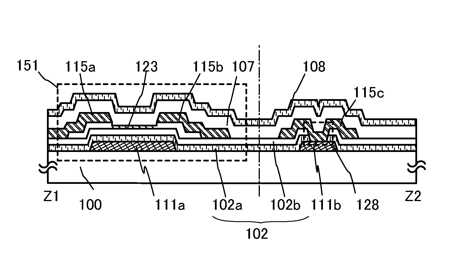
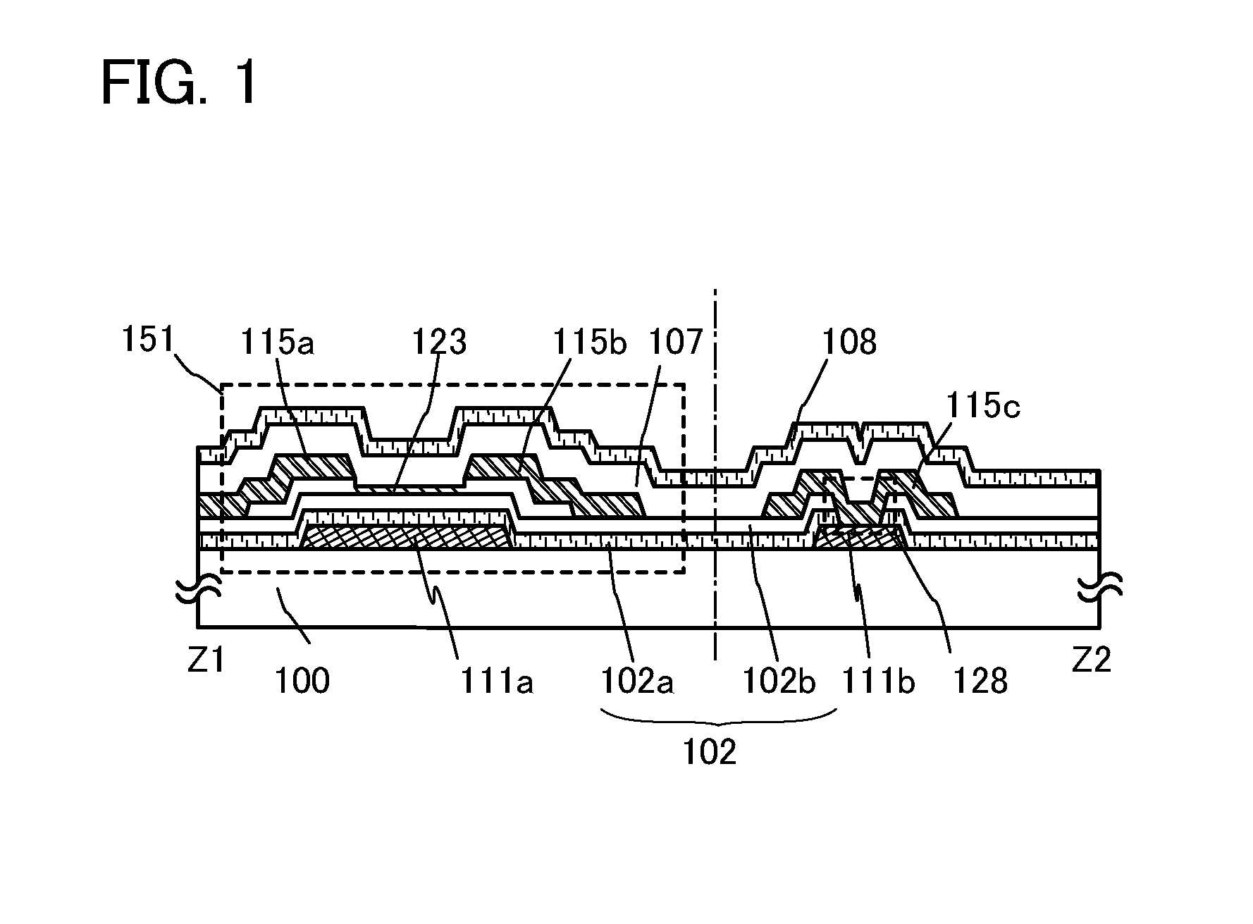
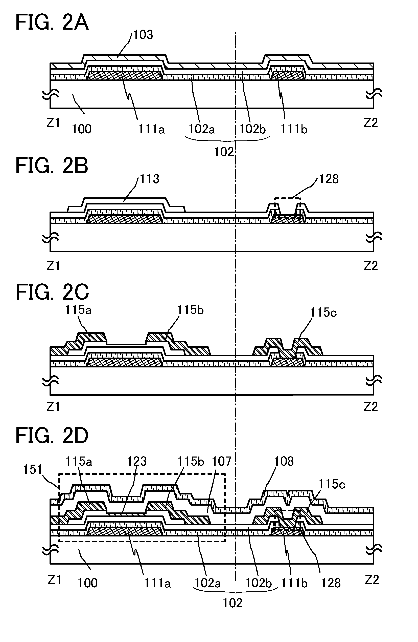
[0041]In this embodiment, a method for manufacturing a semiconductor element is described. Note that in this embodiment, a structure of a thin film transistor illustrated in FIG. 1 and a manufacturing method thereof are described as an example.

[0042]FIG. 1 is a cross-sectional view illustrating a thin film transistor 151 of this embodiment. In the thin film transistor 151, a first wiring layer including a gate electrode 111a and a gate wiring layer 111b is formed over a substrate 100, and a gate insulating layer 102 is formed over the gate electrode 111a and the gate wiring layer 111b. The gate insulating layer 102 is a stack of a first gate insulating layer 102a and a second gate insulating layer 102b. An oxide semiconductor layer 123 is formed over the gate electrode 111a with the gate insulating layer 102 interposed therebetween. A source electrode layer and a drain electrode layer (denoted by 115a and 115b) are formed in a manner that end portions of the source layer and the dra...

embodiment 2

[0116]In this embodiment, an apparatus for successive deposition used for manufacturing a semiconductor element of one embodiment of the present invention and a method for deposition with use of the apparatus are described. Note that in this embodiment, a process of successive deposition is described, and the other process may be performed in accordance with Embodiment 1 to manufacture of a thin film transistor.

[0117]An apparatus for successive deposition 1000 used in this embodiment is illustrated in FIG. 3. The apparatus for successive deposition 1000 includes a load chamber 1110 and an unload chamber 1120. The load chamber 1110 and the unload chamber 1120 are respectively provided with a cassette 1111 which stores a substrate before treatment and a cassette 1121 which stores a substrate after treatment. A first transfer chamber 1100 is provided between the load chamber 1110 and the unload chamber 1120, and is provided with a transfer unit 1101 which transfers a substrate.

[0118]In...

embodiment 3

[0137]In this embodiment, an apparatus for forming an oxide semiconductor layer and a method for forming the oxide semiconductor layer with use of the apparatus are described. Note that in this embodiment, a process of forming the oxide semiconductor layer is described, and the other process may be performed in accordance with Embodiment 1 to manufacture of a thin film transistor.

[0138]A deposition apparatus 2000 used in this embodiment is illustrated in FIG. 4. The deposition apparatus 2000 includes a load chamber 2110 and an unload chamber 2120. The load chamber 2110 and the unload chamber 2120 are respectively provided with a cassette 2111 which stores a substrate before treatment and a cassette 2121 which stores a substrate after treatment. A first transfer chamber 2100 is provided between the load chamber 2110 and the unload chamber 2120, and is provided with a transfer unit 2101 which transfers a substrate.

[0139]In addition, the deposition apparatus 2000 includes a second tran...


PUM


Abstract

An object is to provide a thin film transistor and a method for manufacturing the thin film transistor including an oxide semiconductor with a controlled threshold voltage, high operation speed, a relatively easy manufacturing process, and sufficient reliability. An impurity having influence on carrier concentration in the oxide semiconductor layer, such as a hydrogen atom or a compound containing a hydrogen atom such as H2O, may be eliminated. An oxide insulating layer containing a large number of defects such as dangling bonds may be formed in contact with the oxide semiconductor layer, such that the impurity diffuses into the oxide insulating layer and the impurity concentration in the oxide semiconductor layer is reduced. The oxide semiconductor layer or the oxide insulating layer in contact with the oxide semiconductor layer may be formed in a deposition chamber which is evacuated with use of a cryopump whereby the impurity concentration is reduced.

Description

TECHNICAL FIELD[0001]The present invention relates to semiconductor elements and methods for manufacturing the semiconductor elements. Specifically, the present invention relates to semiconductor elements each including an oxide semiconductor and manufacturing methods thereof.BACKGROUND ART[0002]A thin film transistor (TFT) formed over a flat plate such as a glass substrate, which is typically used in a liquid crystal display device, is generally formed using a semiconductor material such as amorphous silicon or polycrystalline silicon. TFTs using amorphous silicon have low electric field mobility, but can respond to increase in size of glass substrates. On the other hand, TFTs using polycrystalline silicon have high electric field mobility, but need a crystallization step such as laser annealing and are not always adaptable to increase in size of glass substrates.[0003]In contrast, a technique in which a TFT is formed using an oxide semiconductor as a semiconductor material and app...

Claims


Application Information

Patent Timeline
Patent Type & Authority Applications(United States)
IPC IPC(8): H01L29/26H01L21/336
CPCH01L27/1225H01L29/66969H01L21/02565H01L29/7869H01L21/02631H01L29/66742
Inventor YAMAZAKI, SHUNPEISAKATA, JUNICHIROMIYANAGA, AKIHARUSAKAKURA, MASAYUKIKOEZUKA, JUNICHIMARUYAMA, TETSUNORIIMOTO, YUKI
Owner SEMICON ENERGY LAB CO LTD
Why Eureka
Try Eureka