Method and apparatus for improving photovoltaic efficiency

a technology of transparent conductive film and photovoltaic efficiency, which is applied in the direction of sustainable manufacturing/processing, final product manufacturing, vacuum evaporation coating, etc., can solve the problems of reducing the amount of sunlight converted to electricity, reducing the carrier mobility of pv cells, and reducing the photoelectric conversion efficiency. , to achieve the effect of high transmissivity

Inactive Publication Date: 2011-04-21
APPLIED MATERIALS INC
View PDF6 Cites 17 Cited by
  • Summary
  • Abstract
  • Description
  • Claims
  • Application Information

AI Technical Summary

Benefits of technology

[0008]Other embodiments provide a solar cell device with a photoelectric unit, a transmissive conductive layer adjacent to the photoe

Problems solved by technology

Overly high impurities or contaminants of the transparent conductive film often result in high contact resistance at the interface of the transparent conductive film and adjacent films, thereby reducing carrier mobility within the PV cells.
Furthermore, ins

Method used


Image

  • Method and apparatus for improving photovoltaic efficiency
  • Method and apparatus for improving photovoltaic efficiency
  • Method and apparatus for improving photovoltaic efficiency

Examples


Embodiment Construction

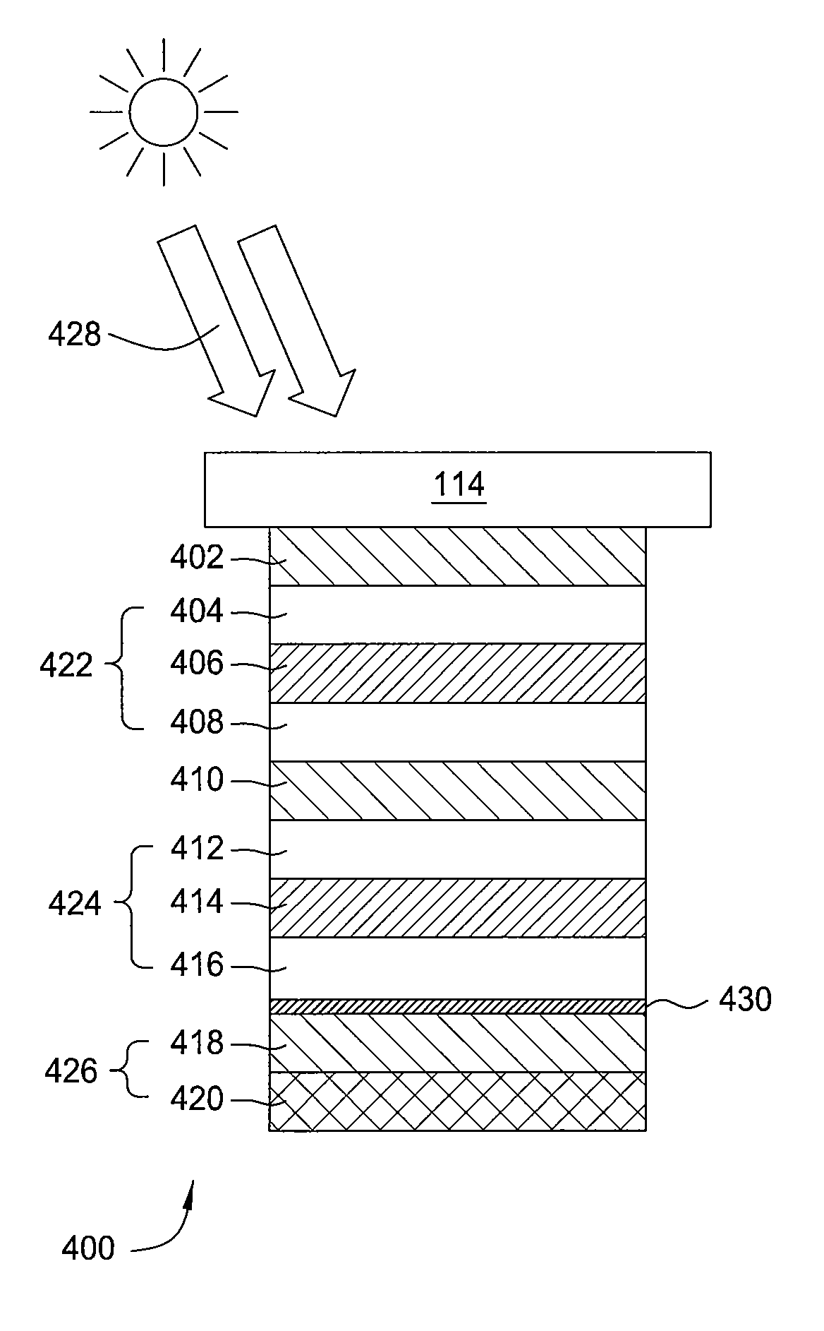
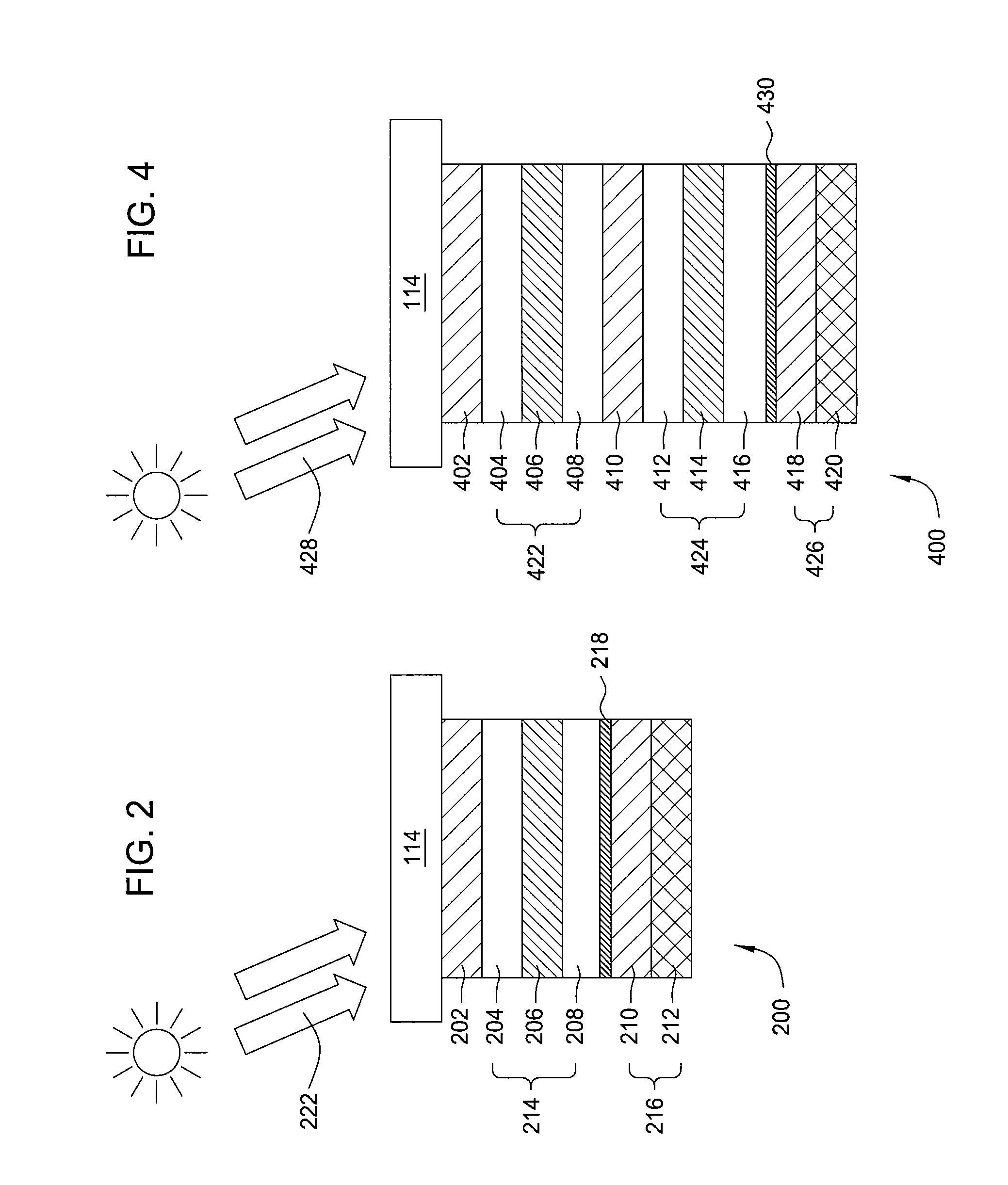
[0015]Embodiments disclosed herein provide methods for forming a transition layer between a semiconductor photoelectric conversion layer and a back contact layer of a solar cell. The transition layer generally reduces recombination of carriers at the interface and / or reflects light back into the photoelectric conversion layer to improve overall efficiency. The back contact layer is generally formed by sputter depositing a transparent conductive layer, such as a transparent conductive oxide layer (TCO layer) on the photovoltaic substrate. The transition layer is formed between the photoelectric conversion layer and the TCO layer, and is preferably a high transmittance layer to avoid introducing absorption. In one embodiment, the TCO layer is sputter deposited by supplying different process gas mixtures along with different target material selections to deposit a TCO layer having a desired dopant concentration formed therein. Composition of the TCO layer at its interface with another ...


PUM

PropertyMeasurementUnit
Fractionaaaaaaaaaa
Percent by atomaaaaaaaaaa
Timeaaaaaaaaaa

Abstract

A method and apparatus for improving efficiency of photovoltaic cells by improving light capture between the photoelectric unit and back reflector is provided. A transition layer is formed at the interface between the photoelectric unit and transmitting conducting layer of the back reflector by adding oxygen, nitrogen, or both to the surface of the photoelectric unit or the interface between the photoelectric unit and the transmitting conducting layer. The transition layer may comprise silicon, oxygen, or nitrogen, and may be silicon oxide, silicon nitride, metal oxide with excess oxygen, metal oxide with nitrogen, or any combination thereof, including bilayers and multi-layers. The sputtering process for forming the transmitting conducting layer may feature at least one of nitrogen and excess oxygen, and may be performed by sputtering at low power, followed by an operation to form the rest of the transmitting conductive layer.

Description

CROSS-REFERENCE TO RELATED APPLICATIONS[0001]This application claims benefit of both U.S. provisional patent application Ser. No. 61 / 252,023, filed Oct. 15, 2009 and U.S. provisional patent application Ser. No. 61 / 301,036, filed Feb. 3, 2010. Each of the aforementioned related patent applications is herein incorporated by reference.FIELD[0002]The present invention relates to methods and apparatus for depositing a transparent conductive film, more specifically, for reactively sputter depositing a transparent conductive film with high transmittance suitable for photovoltaic devices.BACKGROUND[0003]Photovoltaic (PV) devices or solar cells are devices which convert sunlight into direct current (DC) electrical power. PV or solar cells typically have one or more p-n junctions. Each junction comprises two different regions within a semiconductor material where one side is denoted as the p-type region and the other as the n-type region. When the p-n junction of the PV cell is exposed to sun...

Claims


Application Information

Patent Timeline
IPC IPC(8): H01L31/0232H01L31/032C23C14/34
CPCH01L31/03762H01L31/056H01L31/077H01L31/1804H01L31/182H01L31/1824H01L31/1884Y02E10/52Y02E10/545Y02E10/546Y02E10/548C23C14/0084C23C14/027C23C14/086H01L31/022466H01L31/0236H01L31/0368H01L31/03682H01L31/03685Y02E10/547H01L31/076H01L31/022483Y02P70/50
Inventor LE, HIEN-MINH HUUHASSAN, MOHD FADZLI ANWARTANNER, DAVIDWANG, DAPENG
Owner APPLIED MATERIALS INC
Why Eureka
Try Eureka