Semiconductor device

a technology of semiconductor devices and semiconductors, applied in semiconductor devices, capacitors, electrical apparatus, etc., can solve the problems of low on-off ratio of transistors and the difference in stoichiometric composition of oxide semiconductors, and achieve stable operation of circuits, improve aperture ratios, and improve the effect of transistor on-off ratios

Active Publication Date: 2011-04-21
SEMICON ENERGY LAB CO LTD
View PDF43 Cites 232 Cited by
  • Summary
  • Abstract
  • Description
  • Claims
  • Application Information

AI Technical Summary

Benefits of technology

[0013]With one embodiment of the present invention, by forming a circuit by using a transistor that includes a highly-purified oxide semiconductor film, stable operation of the circuit can be obtained. Since off-state current is lowered to less than or equal to 1×10⁻¹³ A, a display device including the above-described circuit does not need to be additionally provided with a capacitor for holding a signal voltage applied to a pixel. That is, in the case where the circuit is applied to a display device, a storage capacitor is unnecessary for each pixel; thus, aperture ratio can be improved.
[0014]With one embodiment of the present invention, a display device including the above-described circuit can hold a fixed state of a pixel (e.g., a state in which an image signal is written); thus, stable operation can be obtained also in the case where a still image is displayed.
[0015]With one embodiment of the present invention, high field-effect mobility and low off-state current can be obtained; thus, a semiconductor device including a memory circuit that is operated favorably without problems and that has low power consumption can be obtained. A semiconductor device including such a memory circuit is particularly effective in the case where a transistor including an oxide semiconductor layer is provided in a pixel of a display device because the semiconductor device including the memory circuit and the pixel can be manufactured over one substrate.

Problems solved by technology

However, a difference from the stoichiometric composition in the oxide semiconductor arises in a thin film formation process.
Such a low on-off ratio of the transistor is due to large off-state current.

Method used


Image

  • Semiconductor device
  • Semiconductor device
  • Semiconductor device

Examples


embodiment 1

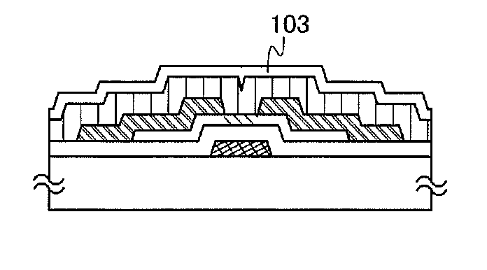
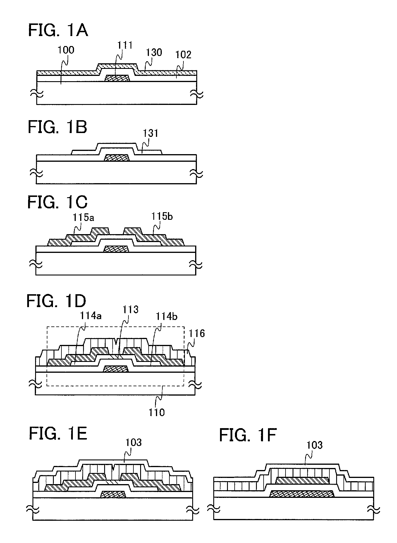
[0047]In this embodiment, a semiconductor device which is one embodiment of the present invention is described.

[0048]First, a transistor which can be used for the semiconductor device of this embodiment is described with reference to FIGS. 1A to 1E.

[0049]A transistor 110 illustrated in FIGS. 1A to 1E is an inverted staggered transistor having a bottom-gate structure.

[0050]Although the transistor 110 is a single-gate transistor, a multi-gate transistor having a plurality of channel formation regions may also be used as necessary.

[0051]First, after a conductive film is formed over a substrate 100 having an insulating surface, a first photolithography step is performed, so that a gate electrode layer 111 is formed. Alternatively, the gate electrode layer 111 may be formed by processing the conductive film with use of a resist mask formed by an inkjet method. In the case of forming a resist mask by an inkjet method, the manufacturing cost can be reduced because a photomask is not used.

[...

embodiment 2

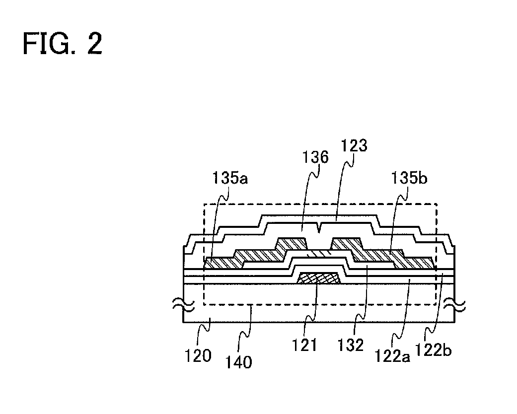
[0166]In this embodiment, a transistor that can be used for the semiconductor device described in Embodiment 1 and is different from the transistor in Embodiment 1 is described.

[0167]FIGS. 10A to 10D illustrate cross-sectional structures of a transistor of this embodiment. A transistor 220 illustrated in FIG. 10D is one mode of a transistor having a bottom-gate structure called a channel-protective type transistor (or a channel-stop type transistor). A process for manufacturing the transistor 220 over a substrate 200 is described below.

[0168]First, a conductive film is formed over the substrate 200 having an insulating surface, and a first photolithography step is performed, so that the conductive film is processed into a gate electrode layer 202.

[0169]The gate electrode layer 202 may be formed using a material similar to that for the gate electrode layer 111 and may have a single-layer structure or a stacked-layer structure of a plurality of layers.

[0170]Note that a resist mask may...

embodiment 3

[0191]In this embodiment, a transistor that can be used for the semiconductor device described in Embodiment 1 and is different from the transistor in Embodiment 1 and Embodiment 2 is described.

[0192]FIGS. 11A to 11D illustrate cross-sectional structures of a transistor of this embodiment. A transistor 320 illustrated in FIG. 11D is one mode of a transistor having a bottom-gate structure. A process for manufacturing the transistor 320 over a substrate 300 is described below.

[0193]First, a conductive film is formed over the substrate 300 having an insulating surface, and a first photolithography step is performed, so that the conductive film is processed into a gate electrode layer 302.

[0194]The gate electrode layer 302 may be formed using a material similar to that for the gate electrode layer 111 and may have a single-layer structure or a stacked-layer structure of a plurality of layers.

[0195]Note that a resist mask may be formed by an inkjet method. In the case of forming a resist...


PUM


Abstract

An object is to provide a memory device including a memory element that can be operated without problems by a thin film transistor with a low off-state current. Provided is a memory device in which a memory element including at least one thin film transistor that includes an oxide semiconductor layer is arranged as a matrix. The thin film transistor including an oxide semiconductor layer has a high field effect mobility and low off-state current, and thus can be operated favorably without problems. In addition, the power consumption can be reduced. Such a memory device is particularly effective in the case where the thin film transistor including an oxide semiconductor layer is provided in a pixel of a display device because the memory device and the pixel can be formed over one substrate.

Description

TECHNICAL FIELD[0001]The present invention relates to semiconductor devices. In particular, the present invention relates to semiconductor devices including memory circuits (e.g., memory devices).BACKGROUND ART[0002]A technique by which transistors are formed using semiconductor thin films formed over a substrate having an insulating surface has been attracting attention. A transistor is used for a display device typified by a liquid crystal television. Silicon is known as a material for a semiconductor thin film applicable to a transistor; however, an oxide semiconductor has attracted attention in recent years.[0003]As a material for the oxide semiconductor, zinc oxide or a material containing zinc oxide as its component is known (e.g., Patent Documents 1 and 2). Further, a transistor formed using an amorphous oxide (oxide semiconductor) having an electron carrier concentration of less than 1018 cm−3 is disclosed (e.g., Patent Document 3).REFERENCEPatent Document[0004][Patent Docum...

Claims


Application Information

Patent Timeline
Patent Type & Authority Applications(United States)
IPC IPC(8): H01L29/786H01L29/78
CPCH01L27/10873H01L27/11H01L27/1108H01L27/1112H01L29/24H01L28/60H01L29/7869G06F15/76H01L27/10805H01L27/1225H10B12/05H10B10/00H10B10/125H10B10/15H01L29/78648H10B12/30H01L27/124H01L27/1255H01L29/41733H01L29/42384H01L29/78696
Inventor YAMAZAKI, SHUNPEITSUBUKU, MASASHINODA, KOSEITOYOTAKA, KOUHEIWATANABE, KAZUNORIHARADA, HIKARU
Owner SEMICON ENERGY LAB CO LTD
Why Eureka
Try Eureka