

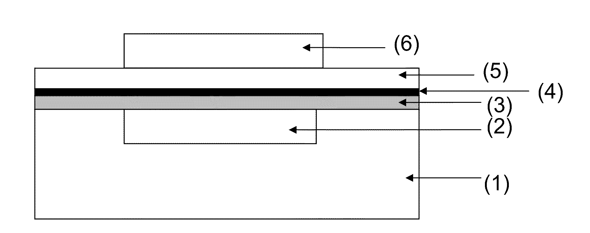
Method for Manufacturing a Low Defect Interface Between a Dielectric and a III-V Compound
a dielectric material and compound technology, applied in the direction of electrical equipment, semiconductor devices, capacitors, etc., can solve the problems of low interface state density, limited integration options, and high carrier mobility
- Summary
- Abstract
- Description
- Claims
- Application Information
AI Technical Summary
Benefits of technology
Problems solved by technology
Method used
Image

Examples
examples
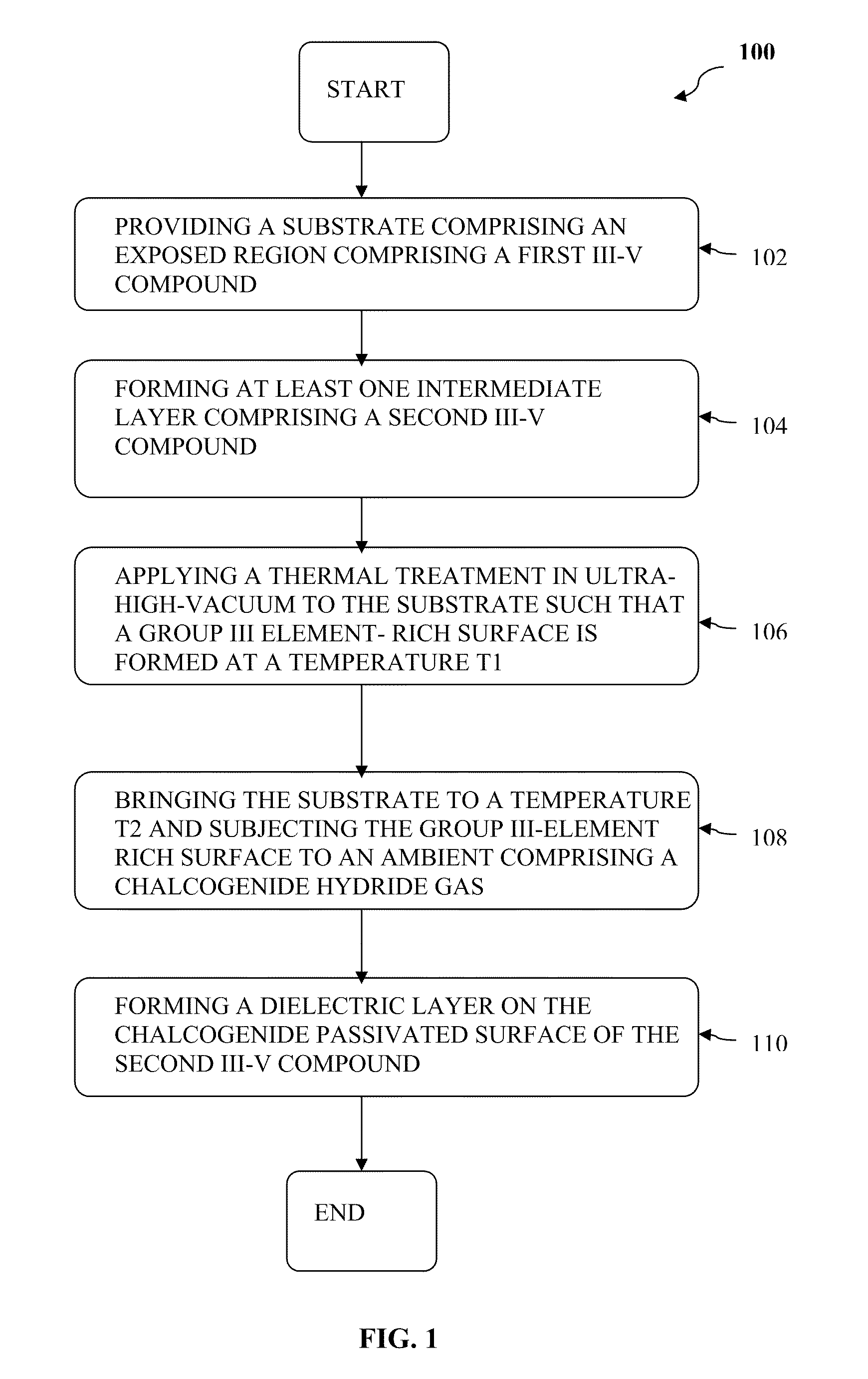
[0170]Growth of Al2O3 / S—GaAs (001) heterostructures was carried out using a molecular beam epitaxy multi-chamber cluster system. The different chambers were connected with a common transfer unit. The chambers and the transfer unit were kept under UHV with a base pressure of 10−11 torr. The base (background) pressure is the pressure in a process chamber before supplying any gas.
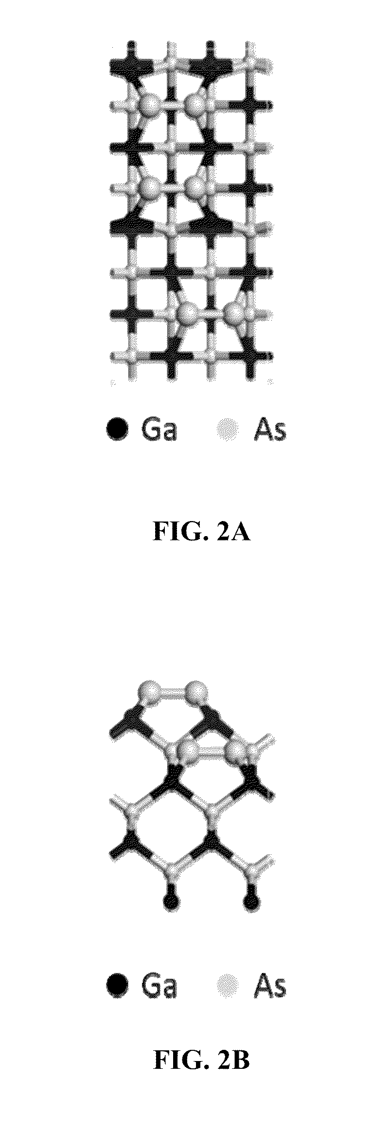
[0171]The intermediate GaAs layers were grown on p-type (001)-oriented GaAs substrates. The GaAs substrates were heated first to 580° C. under As-rich conditions at a pressure of about 2×10⁻⁵ torr, to remove the native oxide. The intermediate GaAs layer had a thickness of about 0.3 μm and were doped with Be with a concentration of about 5×1016 cm−3. The intermediate GaAs layers were grown at 580° C., at a growth rate of about 0.5 mL·s−1 and under As-rich conditions at a pressure of about 1.8×10⁻⁵ torr. As a result of the growth conditions the intermediate GaAs layers show a (2×4) surface reconstruction.
[0172]A...
PUM
| Property | Measurement | Unit |
|---|---|---|
| temperature | aaaaa | aaaaa |
| temperature | aaaaa | aaaaa |
| temperature | aaaaa | aaaaa |
Abstract
Description
Claims
Application Information