

Semiconductor package and method of manufacturing the same
a technology of semiconductor and semiconductor components, applied in the direction of semiconductor/solid-state device details, electrical apparatus, semiconductor devices, etc., can solve the problems of destroying the circuit elements formed in the chip, reducing the size of the chip, and prone to static electricity incident, etc., to reduce power consumption
- Summary
- Abstract
- Description
- Claims
- Application Information
AI Technical Summary
Benefits of technology
Problems solved by technology
Method used
Image


Examples
first embodiment
[0044]A first embodiment of the present invention will be described below with reference to the attached drawings.
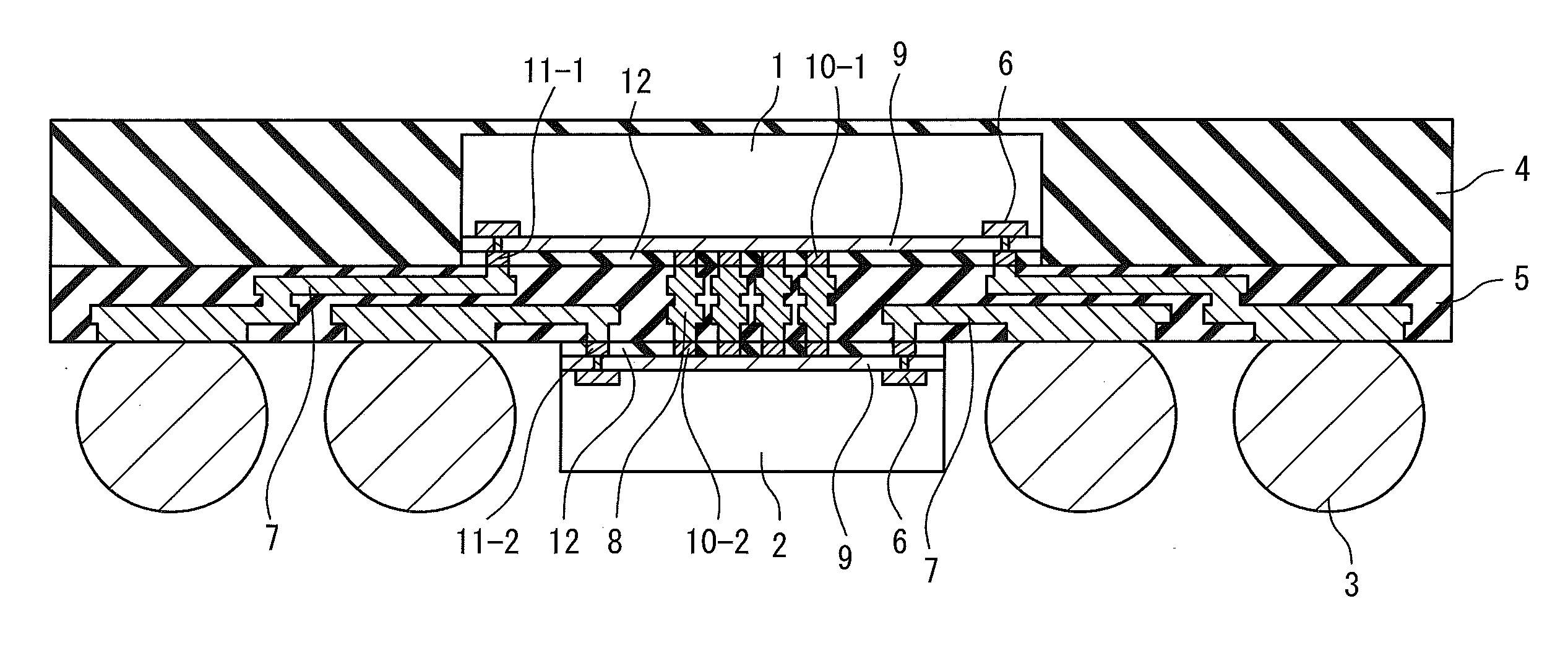
[0045]FIG. 1 is a schematic cross-sectional view showing a semiconductor package according to the present embodiment. As shown in FIG. 1, the semiconductor package has a package substrate 5 (interposer), a first chip 1, a second chip 2 and a sealing body 4.
[0046]The package substrate 5 is a substrate for mounting the first chip 1 and the second chip 2. The package substrate 5 is exemplified by a glass epoxy substrate in which Cu interconnections are formed, a polyimide substrate in which Cu interconnections are formed and the like. The first chip 1 is mounted on a principal surface of the package substrate 5. The second chip 2 is mounted on a back surface of the package substrate 5. Moreover, an internal-connecting interconnection 8 for electrically connecting the first chip 1 and the second chip 2 with each other is formed in the package substrate 5. In addition, extern...
second embodiment
[0077]Next, a second embodiment of the present invention will be described. FIG. 10 is a schematic cross-sectional view showing the semiconductor package according to the present embodiment. In the present embodiment, both of the first chip 1 and the second chip 2 are mounted on the principal surface of the package substrate 5. The other features are the same as those in the first embodiment, and an overlapping description will be omitted as appropriate.
[0078]As shown in FIG. 10, both of the first chip 1 and the second chip 2 are mounted on the principal surface of the package substrate 5 and are sealed by the sealing body 4.
[0079]A method of manufacturing the semiconductor package according to the present embodiment will be described below.
[0080]As shown in FIG. 11, the package substrate 5 is formed on the support 17. The package substrate 5 has the internal-connecting interconnection 8 and the external-connecting interconnection 7. Then, the first chip 1 and the second chip 2 are ...
third embodiment
[0086]Next, a third embodiment of the present invention will be described. In the present embodiment, the first chip 1 is mounted on a principal surface of the second chip 2. The other features are the same as those in the above-described embodiments, and an overlapping description will be omitted as appropriate.
[0087]FIG. 15 is a schematic cross-sectional view showing the semiconductor package according to the present embodiment.
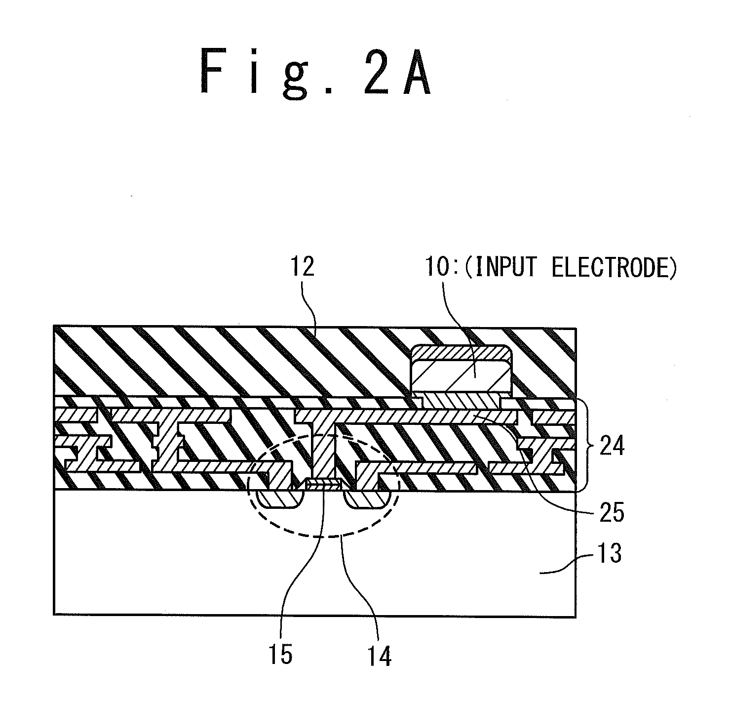
[0088]As shown in FIG. 15, the second chip 2 is mounted on a principal surface of the package substrate 5. Circuits are formed on a principal surface of the second chip 2. That is, the principal surface of the second chip 2 is a circuit formation surface 9-2. Specifically, the external electrode group 11-2 electrically connected to the ESD protection element 6 and the internal electrode group 10-2 that is not electrically connected to the ESD protection element 6 are formed on the circuit formation surface 9-2 of the second chip 2. The external electrode gr...
PUM
 Abstract
Description
Claims
Application Information