Semiconductor light emitting apparatus and light source apparatus using the same

a technology of semiconductors and light sources, applied in the direction of lighting and heating apparatus, luminescent compositions, chemistry apparatus and processes, etc., can solve the problems of reducing the photon conversion efficiency, increasing the lattice vibration in the solid, and generating heat, so as to ensure high wave conversion efficiency and ensure high-power output. , the effect of excellent heat dissipation

Inactive Publication Date: 2011-04-21
PANASONIC CORP
View PDF22 Cites 24 Cited by
  • Summary
  • Abstract
  • Description
  • Claims
  • Application Information

AI Technical Summary

Benefits of technology

[0014]The semiconductor light emitting apparatus according to the present invention has a wavelength converter that is an inorganic compact. By virtue of this, excellent heat dissipation is achieved.
[0015]In addition, since the amount of Ce3+ substituting part of the constituent element group is limited to 1 atomic % or less, the wave conversion efficiency is ensured to be high (absolute quantum efficiency is 80% or higher) and thus high-power output is ensured. The semiconductor light emitting apparatus is enabled to emit more illumination light adjusted suitably for general illumination purpose. The present invention achieves to provide a high-power semiconductor light emitting apparatus suitable for general illumination purpose.

Problems solved by technology

Unfortunately, however, to increase the output power of a semiconductor light emitting apparatus means to increase the fluorescent excitation light emitted by the LED chip, which leads to heat generation due to the energy loss (Stokes loss) associated with the wavelength conversion by the phosphor.
The heat builds up in the resin phosphor layer to elevate the temperature of the resin phosphor layer, which increases the lattice vibrations in the solid to reduce the photon conversion efficiency.
The physical properties of the transparent resin are adversely affected to reduce the optical output and reliability (such as the reduction of light transmittance).

Method used


Image

  • Semiconductor light emitting apparatus and light source apparatus using the same
  • Semiconductor light emitting apparatus and light source apparatus using the same
  • Semiconductor light emitting apparatus and light source apparatus using the same

Examples


embodiment 1

Preferred embodiment 1

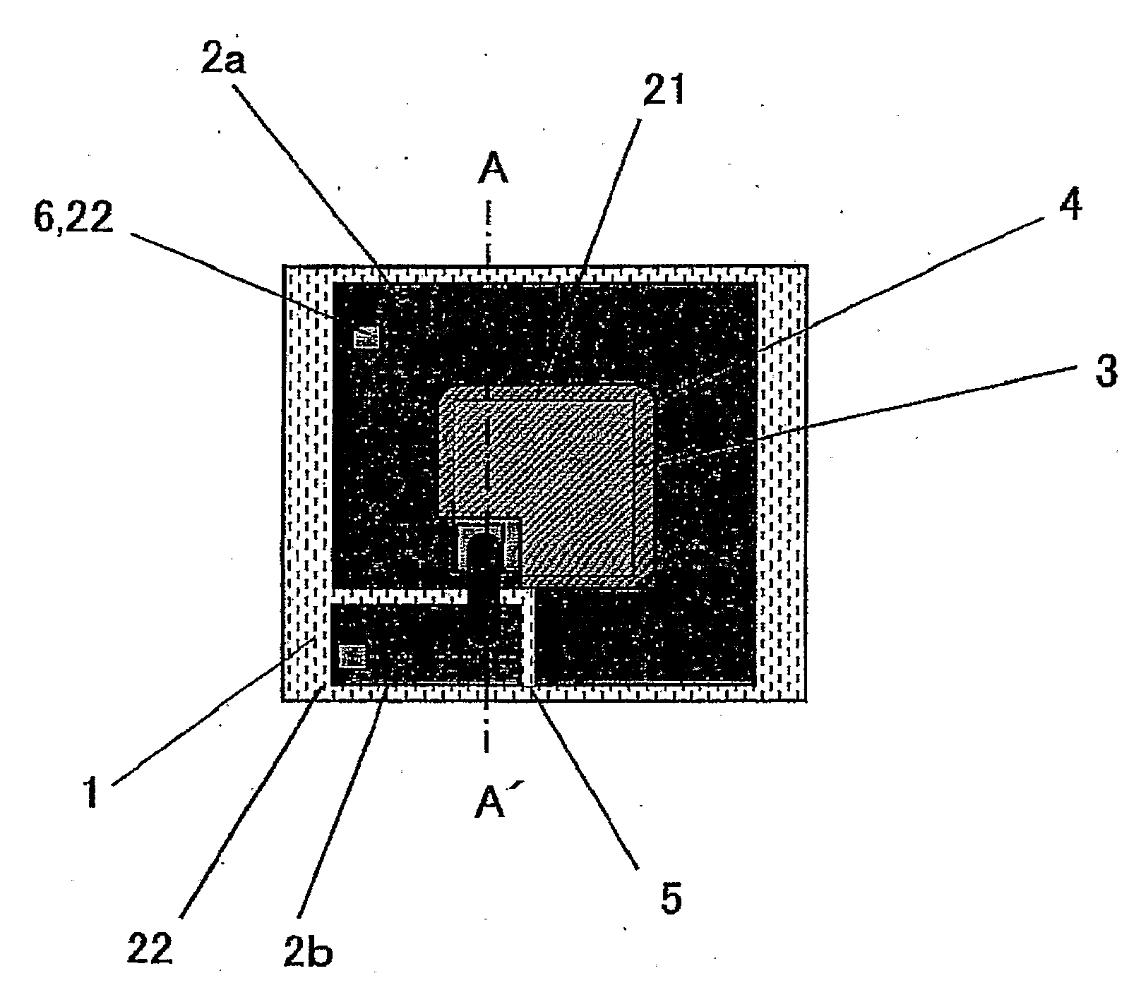
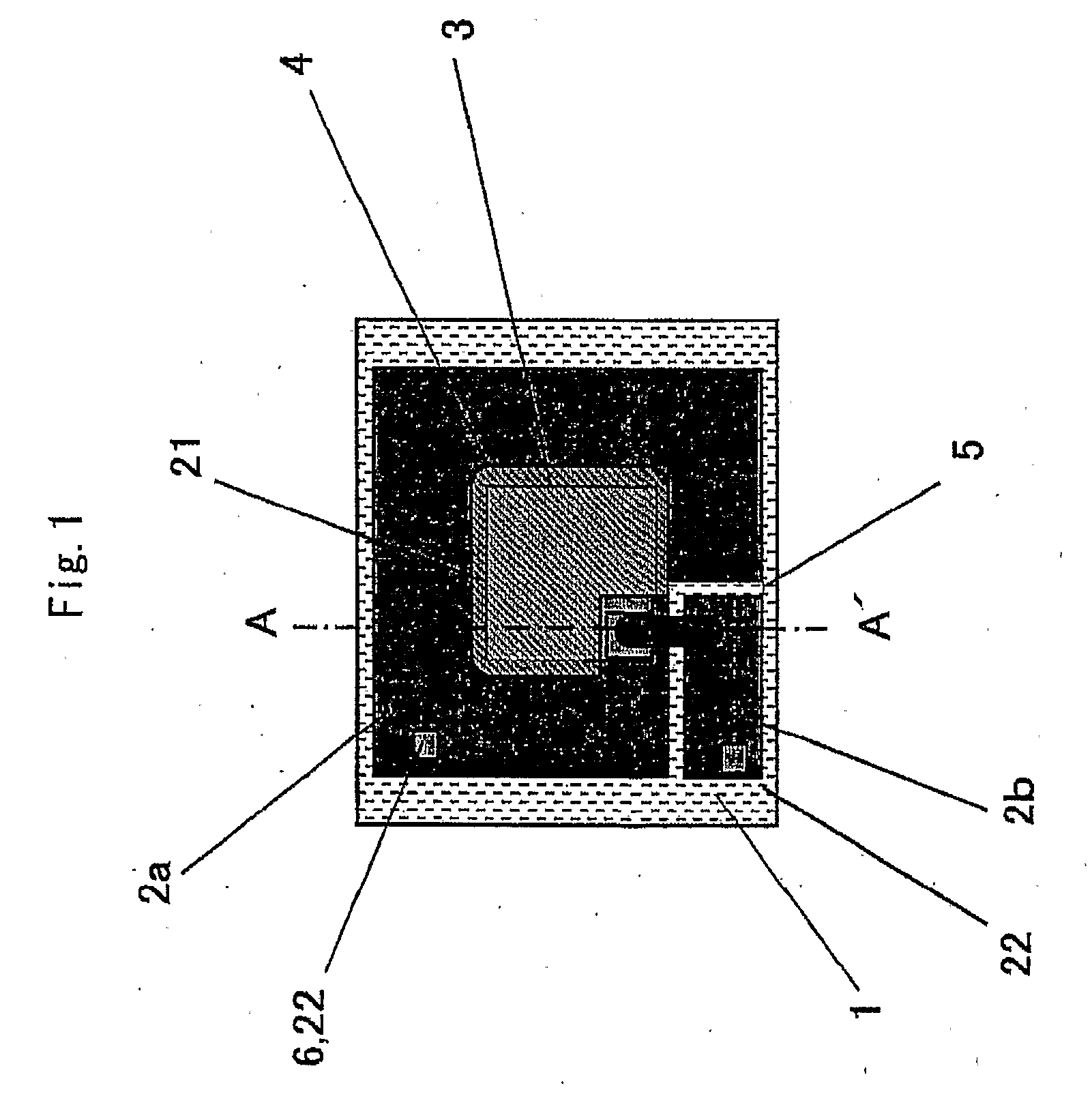
[0304]The following is more detailed description, including description of the positional arrangement, of the solid-state light emitting device 3 and the wavelength converter 4 having the wavelength conversion layer 4a.

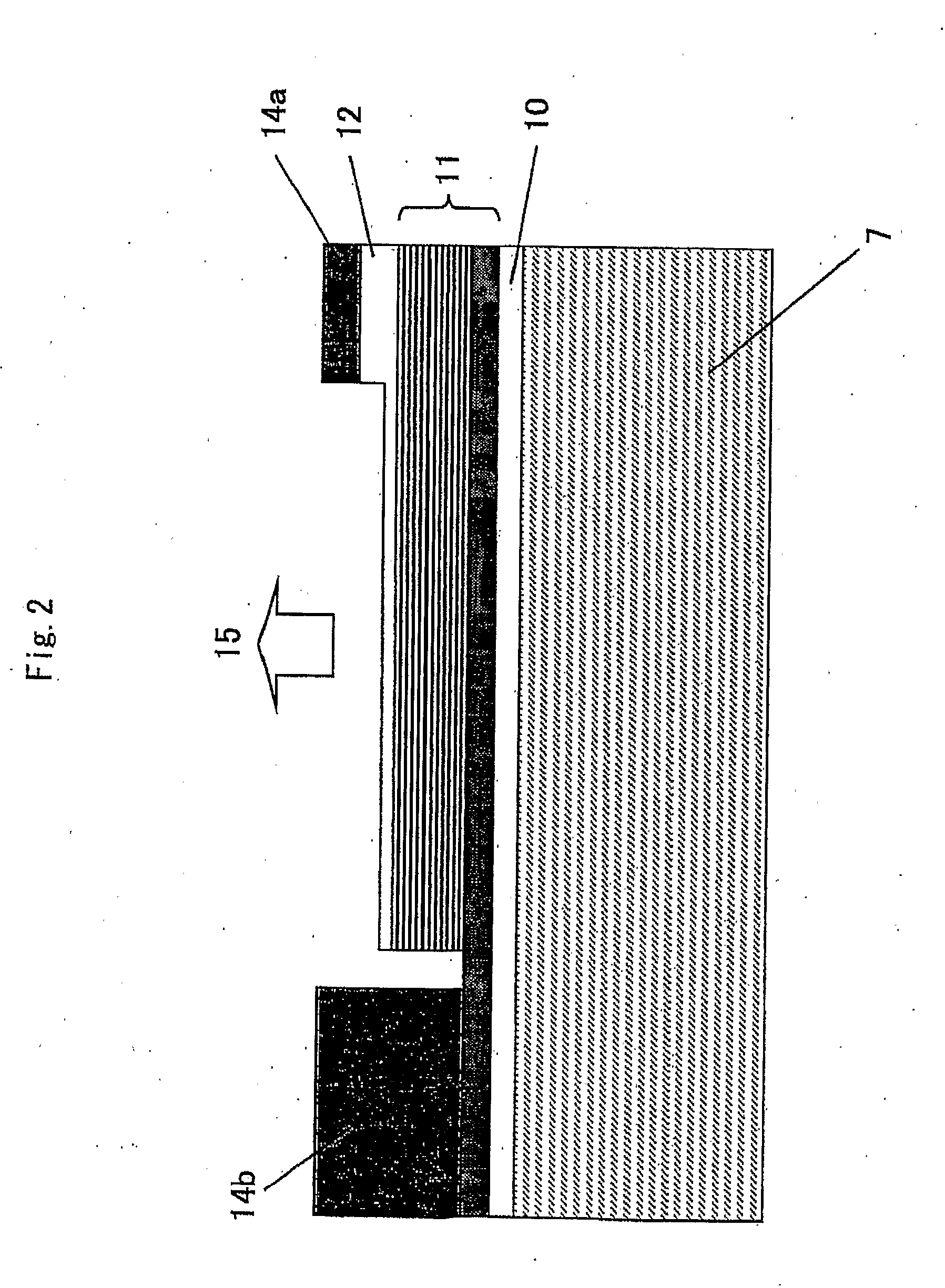
[0305]FIG. 12 is a cross-sectional side view of the exemplary semiconductor light emitting apparatus shown in FIG. 1, taken along the line A-A′.

[0306]As shown in FIG. 12, the semiconductor light emitting apparatus according to one embodiment of the present invention at least includes the solid-state light emitting device 3 and the wavelength converter 4. The wavelength converter 4 is an inorganic compact having the transparent wavelength conversion layer 4a. The wavelength conversion layer 4a at least contains an inorganic phosphor (not shown) that absorbs the primary light (not shown) emitted by the solid-state light emitting device 3 and emits light at a longer wavelength than the primary light. The thickness of the wavelength conversion layer...

embodiment 2

[0471]FIGS. 16 and 17 are cross-sectional side views each showing, an example of a headlight apparatus (such as a projection light source or a vehicle headlight) configured by employing a semiconductor light emitting apparatus according to the present invention.

[0472]As shown in. FIGS. 16 and 17, the light source apparatus according to the preferred embodiment 2 of the present invention is configured with the semiconductor light emitting apparatus 27 according to the preferred embodiment 1. In one preferable embodiment, the light source apparatus at least includes an external heat dissipator 29 in combination with the semiconductor light emitting apparatus 27.

[0473]This configuration provides a small and compact light source apparatus that emits beam light.

[0474]In FIGS. 16 and 17, the semiconductor light emitting apparatus 27 is the semiconductor light emitting apparatus described in the preferred embodiment 1 and emits output light 28 in response to electrical power supply.

[0475]T...


PUM

PropertyMeasurementUnit
wavelength regionaaaaaaaaaa
correlated color temperatureaaaaaaaaaa
thicknessaaaaaaaaaa

Abstract

A semiconductor light emitting apparatus includes a solid-state light emitting device and a wavelength converter that converts primary light emitted by the solid-state light emitting device into secondary light at a loner-wavelength. The wavelength converter is an inorganic compact that includes a transparent wavelength conversion layer containing phosphor having a garnet crystal structure. The phosphor contains a constituent element group composed of at least one element selected from the group consisting of Mg, Ca, Sr, Ba, Y, La, Gd, Tb, and Lu. Part of the constituent element group is substituted by Ce3+ and the amount of Ce+ is 1 atomic % less of the entire constituent element group. As a result, a high-power and highly reliable semiconductor light emitting apparatus suitable as a point light source is provided. In addition, such a semiconductor light emitting apparatus is manufactured through a simple application of traditionally used practical technicians.

Description

TECHNICAL FIELD[0001]The present invention relates to semiconductor light emitting apparatuses used as point light, sources for vehicle headlights and projection light sources and also relates to light source apparatuses using such a semiconductor light emitting apparatus.BACKGROUND ART[0002]Example of the semiconductor light emitting apparatuses above include a white LED having a solid-state light emitting device and a wavelength converter that converts the primary light emitted by the solid-state light emitting device into loner-wavelength light. Commonly used in such a white LED (hereinafter, “LED chip” or simply “chip”) is a light emitting diode having a light-emitting layer of a InGaN-based compound semiconductor. An example of the wavelength converter is a resin phosphor layer made from a phosphor powder (phosphor particles) dispersed in a transparent resin.[0003]In recent years, there is a growing demand for higher-output semiconductor light emitting apparatuses. Unfortunatel...

Claims


Application Information

Patent Timeline
Patent Type & Authority Applications(United States)
IPC IPC(8): F21V5/00H01L33/50
CPCC04B35/44C04B2235/3224H01L2224/73265H01L2224/48091H01L2224/45144C04B2235/3225C04B2235/3229C04B2235/764C04B2235/9661C09K11/7774H01L33/502H01L33/505H01L33/644H01L2924/00014H01L2924/00H01L2924/12044
Inventor ISHIMORI, ATSUYOSHIOSHIO, SHOZOUENO, YASUHARUTANIMOTO, NORIYASU
Owner PANASONIC CORP
Why Eureka
Try Eureka