Plasma processing apparatus and plasma processing method

a plasma processing apparatus and plasma technology, applied in the field of techniques, can solve the problems of increasing the cost insufficient uniform plasma density on the substrate obtained by merely using a typical rf antenna, and remarkably increasing the configuration of rf power supply units, so as to achieve the effect of improving the uniformity of the plasma process

Active Publication Date: 2011-04-28
TOKYO ELECTRON LTD
View PDF22 Cites 20 Cited by
  • Summary
  • Abstract
  • Description
  • Claims
  • Application Information

AI Technical Summary

Benefits of technology

[0018]In the plasma processing method of the present invention, with the above technique, especially, where the correction coil that can be coupled with the RF antenna by the electromagnetic induction is provided outside the processing chamber so as to be in parallel with the RF antenna; and the distance between the RF antenna and the correction coil is variably controlled while maintaining the correction coil in parallel with the RF antenna, it is possible to stably obtain in a standardized manner the effect of the correction coil on the RF magnetic field generated around the antenna conductor by the RF current f

Problems solved by technology

However, the uniformity of the plasma density on the substrate that is obtained by merely using a typical RF antenna is generally insufficient for the plasma process.
However, the first method of the above-described RF antenna dividing methods is disadvantageous in that the requirement for a plurality of RF power supplies and a plurality of matchers corresponding thereto makes the configuration of the RF power supply unit complex and increases the costs remarkably.
The second method is rarely used due to the poor controllability.
To be specific, it is difficult to control the division ratio only by the additional circuit because each of impedances of the antenna segments is affected by the impedances of the plasma as well as other antennas segments.
Since, however, the effect of the passive antenna has not been su

Method used


Image

  • Plasma processing apparatus and plasma processing method
  • Plasma processing apparatus and plasma processing method
  • Plasma processing apparatus and plasma processing method

Examples


first embodiment

[0048]A first embodiment of the present invention will be described with reference to FIGS. 1 to 8.

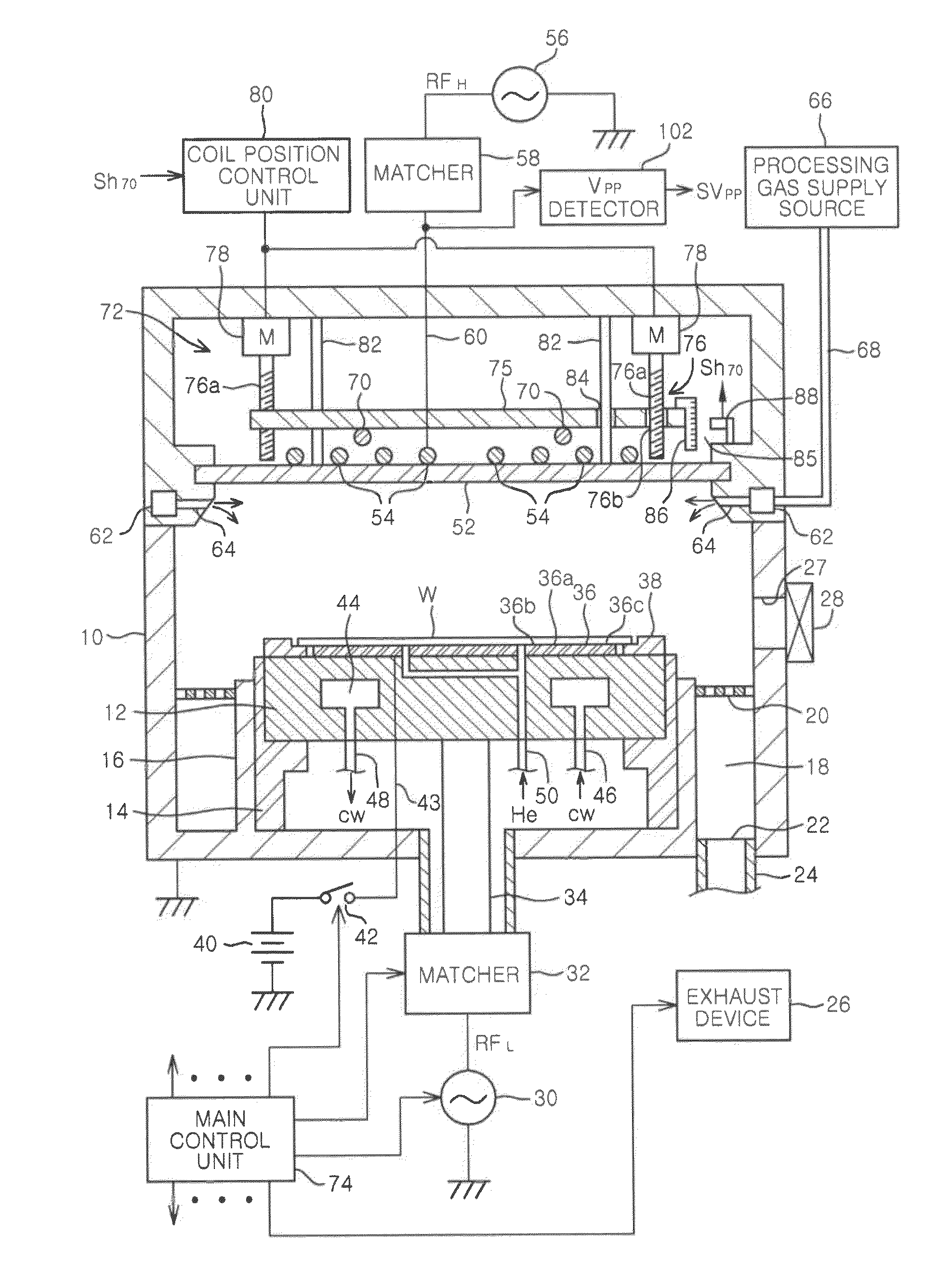
[0049]FIG. 1 shows a configuration of an inductively coupled plasma processing apparatus in accordance with the first embodiment of the present invention. The inductively coupled plasma processing apparatus is configured as a plasma etching apparatus using a planar coil type RF antenna, and includes a cylindrical vacuum chamber (processing chamber) 10 made of a metal, e.g., aluminum, stainless steel or the like. The chamber 10 is frame-grounded.

[0050]In the inductively coupled plasma etching apparatus, various units having no involvement in plasma generation will be described first.

[0051]At a lower central portion of the chamber 10, a circular plate-shaped susceptor 12 for mounting thereon a target substrate, e.g., a semiconductor wafer W as a substrate supporting table is horizontally arranged. The susceptor 12 also serves as an RF electrode. The susceptor 12, which is made of, e.g., ...

second embodiment

[0107]Hereinafter, a second embodiment of the present invention will be described with reference to FIGS. 9 to 14.

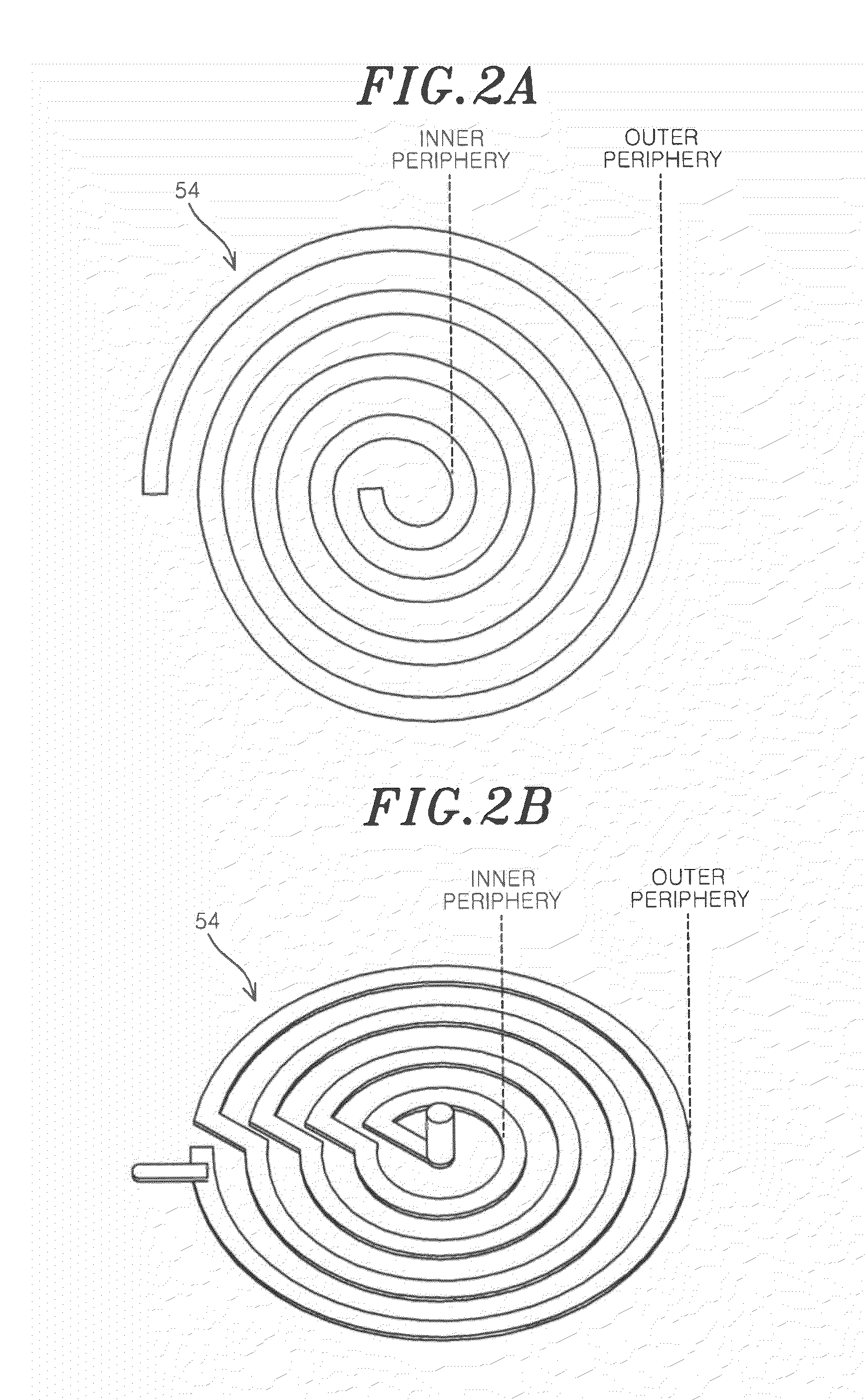
[0108]In a plasma etching apparatus of the second embodiment, the uniformity of the radial distribution of the plasma density around the susceptor 12 can be improved; the electromagnetic correction of the RF magnetic field generated by the RF antenna 54 can be performed by the correction coil 90; and the vertical position of a correction coil 90 having a capacitor can be variably controlled by the antenna-coil distance control unit 72.

[0109]Hereinafter, the configuration and the operation of the correction coil 90 having a capacitor as a major feature of the inductively coupled plasma etching apparatus will be described.

[0110]As shown in FIG. 9, the correction coil 90 is formed of a single- or a multi-wound coil having both open ends with a cutout portion (gap) G therebetween, and a fixed capacitor 94 is provided at the cutout portion G. The fixed capacitor 94, as will b...

third embodiment

[0126]As for the configuration and function of a correction coil and its peripheral units in accordance with a third embodiment of the prevent invention, as shown in FIG. 15, the correction coil of the present invention may be preferably provided with a coil rotation mechanism 180 for rotating or rotatably displacing the correction coil 90 having a capacitor in a concentric positional relationship with the RF antenna 54. The coil rotation mechanism 180 includes, e.g., an insulating substrate support plate 182 for horizontally supporting the correction coil 90 in a concentric positional relationship with the RF antenna 54, a stepping motor 186 coupled with the central portion of the substrate support plate 182 through a vertical rotation shaft 184, and a rotation control unit 188 for controlling the rotation direction, the rotation speed or the rotation angle of the correction coil 90 by using the stepping motor 186. A speed reduction mechanism (not shown) may be provided between the...


PUM

PropertyMeasurementUnit
Diameteraaaaaaaaaa
Magnetic fieldaaaaaaaaaa
Distanceaaaaaaaaaa

Abstract

A plasma processing apparatus includes: a processing chamber including a dielectric window; a coil-shaped RF antenna, provided outside the dielectric window; a substrate supporting unit, provided in the chamber, for mounting thereon a target substrate; a processing gas supply unit for supplying a processing gas to the chamber; and an RF power supply unit for supplying an RF power to the RF antenna to generate a plasma of the processing gas by an inductive coupling in the chamber. The apparatus further includes a correction coil, provided at a position outside the chamber where the correction coil is to be coupled with the RF antenna by an electromagnetic induction, for controlling a plasma density distribution in the chamber; and an antenna-coil distance control unit for controlling a distance between the RF antenna and the correction coil while supporting the correction coil substantially in parallel with the RF antenna.

Description

CROSS-REFERENCE TO RELATED APPLICATIONS [0001]This application claims priority to Japanese Patent Application Nos. 2009-245988 and 2009-245991 filed on Oct. 27, 2009 and 2010-215111 filed on Sep. 27, 2010 and U.S. Provisional Application Nos. 61 / 265545 and 61 / 265523 filed on Dec. 1, 2009, the entire contents of which are incorporated herein by reference.FIELD OF THE INVENTION [0002]The present invention relates to a technique for performing a plasma process on a target substrate to be processed; and, more particularly, to an inductively coupled plasma processing apparatus and a plasma processing method therefor.BACKGROUND OF THE INVENTION[0003]In the manufacturing process of a semiconductor device or a flat panel display (FPD), a plasma is widely used in a process such as etching, deposit, oxidation, sputtering or the like since it has a good reactivity with a processing gas at a relatively low temperature. In such plasma process, the plasma is mostly generated by a radio frequency ...

Claims


Application Information

Patent Timeline
IPC IPC(8): C23F1/08C23C16/455C23C16/458C23C16/505C23F1/00
CPCH01J37/321H01L21/31138H01L21/31122H01L21/31116H01L21/3065H01L21/31H05H1/46
Inventor YAMAZAWA, YOHEIKOSHIMIZU, CHISHIOSAITO, MASASHIDENPOH, KAZUKIYAMAWAKU, JUNIIZUKA, HACHISHIRO
Owner TOKYO ELECTRON LTD
Why Eureka
Try Eureka