

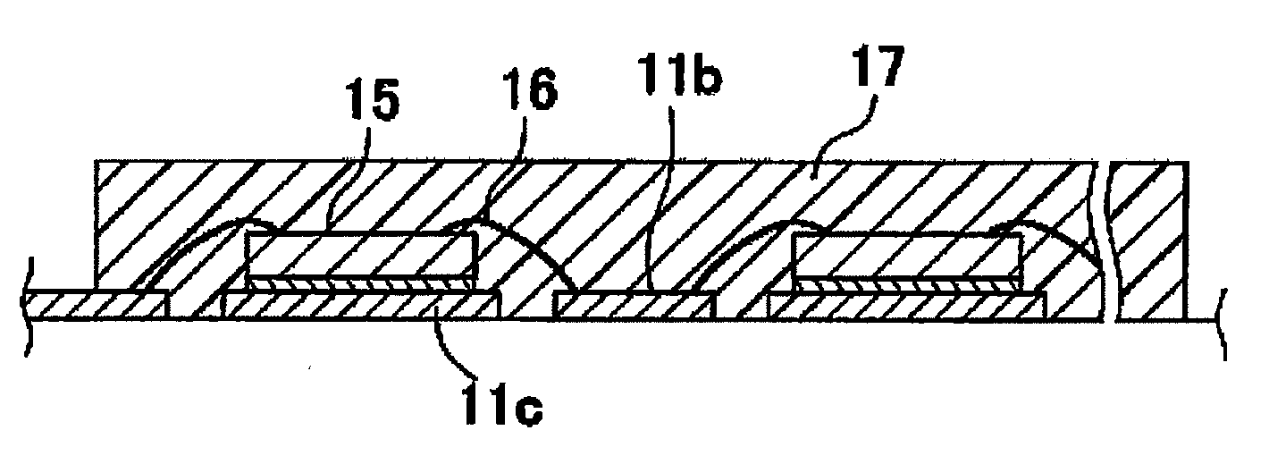
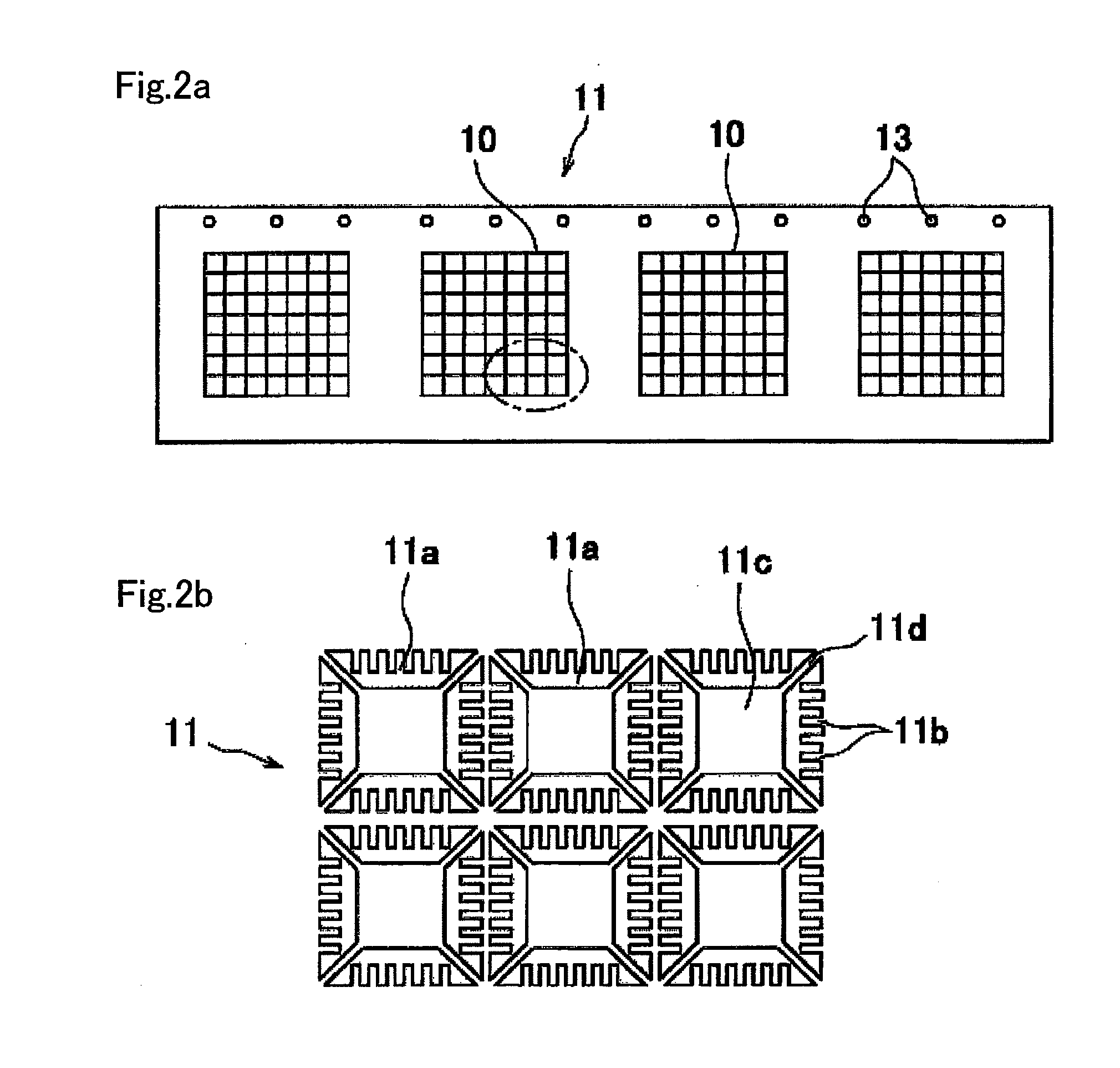
Adhesive tape for resin-encapsulating and method of manufacture of resin-encapsulated semiconductor device
a technology of adhesive tape and resin encapsulation, which is applied in the direction of film/foil adhesives, synthetic resin layered products, transportation and packaging, etc., can solve the problems of resin leakage and achieve the effect of improved productivity and efficient prevention of resin leakag
- Summary
- Abstract
- Description
- Claims
- Application Information
AI Technical Summary
Benefits of technology
Problems solved by technology
Method used
Image

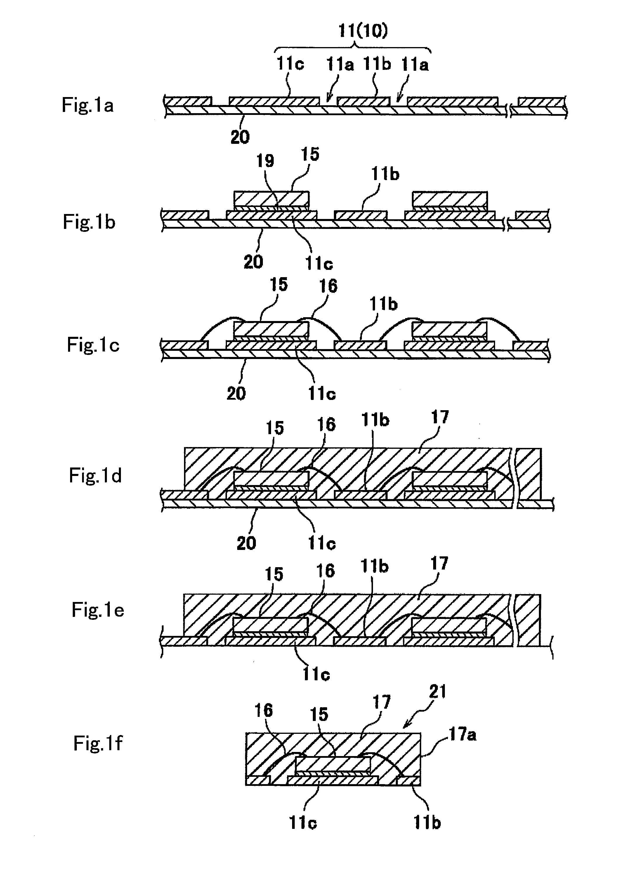
Examples
example 1
[0102]A 25 μm polyimide film (Kapton 100H, coefficient of linear expansion 2.7×10⁻⁵ / K, Tg: 402° C., Du Pont-Toray Co., Ltd.) was used as a base material layer. 2.5 parts of a platinum catalyst was added to 100 parts of a silicon-base adhesive agent (SD4584 manufactured by Dow Corning Toray Co., Ltd.), and coated and dried on one surface of the base material layer to thereby obtain a heat-resistant adhesive tape having an adhesive agent layer of thickness about 6 μm (total film thickness about 31 μm).
example 2
[0103]A 12.5 μm polyimide film (Kapton 50H, coefficient of linear expansion 2.7×10⁻⁵ / K, Tg: 402° C., Du Pont-Toray Co., Ltd.) was used as a base material layer. The silicon-base adhesive agent was used, and obtained a heat-resistant adhesive tape having an adhesive agent layer of thickness about 8 μm (total film thickness about 30.5 μm), in the same manner as Example 1.
example 3
[0104]A 25 μm polyethylene terephthalate film (Lumirror S10, coefficient of linear expansion 1.2×10⁻⁵ / K, Tg: 67° C., Toray Industries Inc.) was used as a base material layer. To 100 parts of polymer made of butyl acrylate-ethyl acrylate-acrylic acid (butyl acrylate: ethyl acrylate: acrylic acid=70 parts: 30 parts: 40 parts) were added 3 parts of isocyanate cross linking agent (trade name “Coronate L,” made by Nippon Polyurethane Industry), 2 parts of epoxy cross linking agent (trade name “tetrad C,” made by Mitsubishi gas chemical company, Inc.) and toluene, and mixed and stirred to prepare an adhesive solution.
[0105]The obtained adhesive solution was coated and dried on one surface of the base material layer to thereby obtain a heat-resistant adhesive tape having an adhesive agent layer of thickness about 10 μm (total film thickness about 35 μm).
PUM
| Property | Measurement | Unit |
|---|---|---|
| Temperature | aaaaa | aaaaa |
| Thickness | aaaaa | aaaaa |
| Thickness | aaaaa | aaaaa |
Abstract
Description
Claims
Application Information