Method for manufacturing semiconductor device

a manufacturing method and semiconductor technology, applied in semiconductor devices, digital storage, instruments, etc., can solve the problems of difficult to reduce a cost the processing technique which meets the conditions required for manufacturing a semiconductor device with the use of an oxide semiconductor has not been established, and the major portion of an oxide semiconductor layer including such an expensive metal which is deposited is removed and wasted, so as to improve the performance of the semiconductor device, the effect of improving throughput and miniaturizing the semiconductor devi

Active Publication Date: 2011-05-19
SEMICON ENERGY LAB CO LTD
View PDF102 Cites 116 Cited by
  • Summary
  • Abstract
  • Description
  • Claims
  • Application Information

AI Technical Summary

Benefits of technology

[0011]Further, a rare metal such as indium is used for an oxide semiconductor. In a conventional processing technique including etching, the major portion of an oxide semiconductor layer including such an expensive metal which is deposited is removed and wasted. Therefore, it is difficult to reduce a cost for manufacturing a semiconductor device in which an oxide semiconductor is used by the conventional processing technique. In addition, measure against problems in resource saving is required.
[0026]According to an embodiment of the present invention disclosed, the island-shaped oxide semiconductor layer functioning as an active layer and the conductive layer covering the island-shaped oxide semiconductor layer are processed by dry etching, whereby the semiconductor device can be miniaturized and performance of the semiconductor device is improved. Further the oxide semiconductor layer above the gate insulating layer is processed by wet etching into an island-shaped oxide semiconductor, so that throughput can be improved.
[0027]In addition, etching of the oxide semiconductor layer over the gate insulating layer, which does not need control of the etching relatively, is performed by wet etching and channel etching which needs miniaturization and control of etching is performed by dry etching, so that throughput can be improved in the whole manufacturing process and higher performance of the semiconductor device can be achieved.
[0028]Further, wet etching is employed when the oxide semiconductor layer is processed so as to have an island shape, and a material such as indium included in the oxide semiconductor layer is collected from a wasted solution after the etching and reused, so that the resources can be effectively used and cost can be reduced.

Problems solved by technology

However, a processing technique which satisfies conditions required for manufacturing a semiconductor device with the use of an oxide semiconductor has not been established yet.
In a conventional processing technique including etching, the major portion of an oxide semiconductor layer including such an expensive metal which is deposited is removed and wasted.
Therefore, it is difficult to reduce a cost for manufacturing a semiconductor device in which an oxide semiconductor is used by the conventional processing technique.

Method used


Image

  • Method for manufacturing semiconductor device
  • Method for manufacturing semiconductor device
  • Method for manufacturing semiconductor device

Examples


embodiment 1

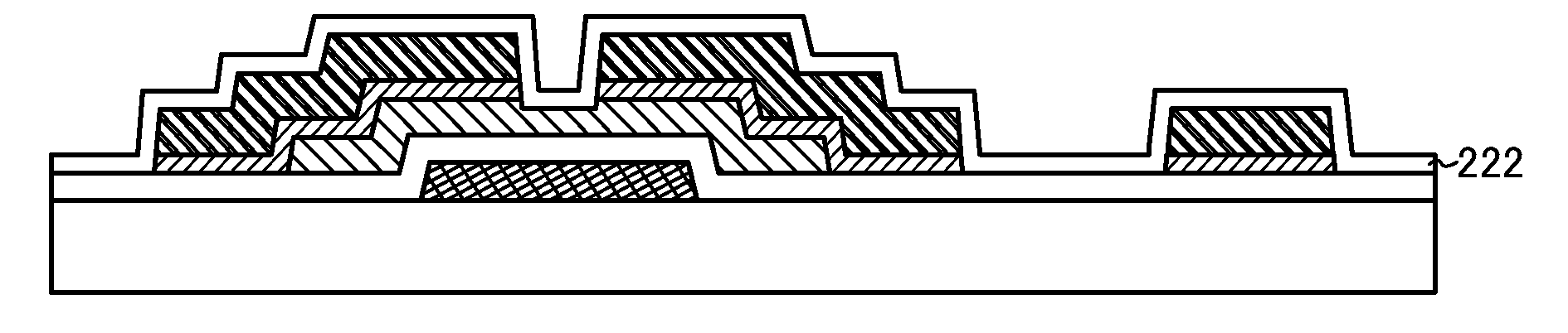
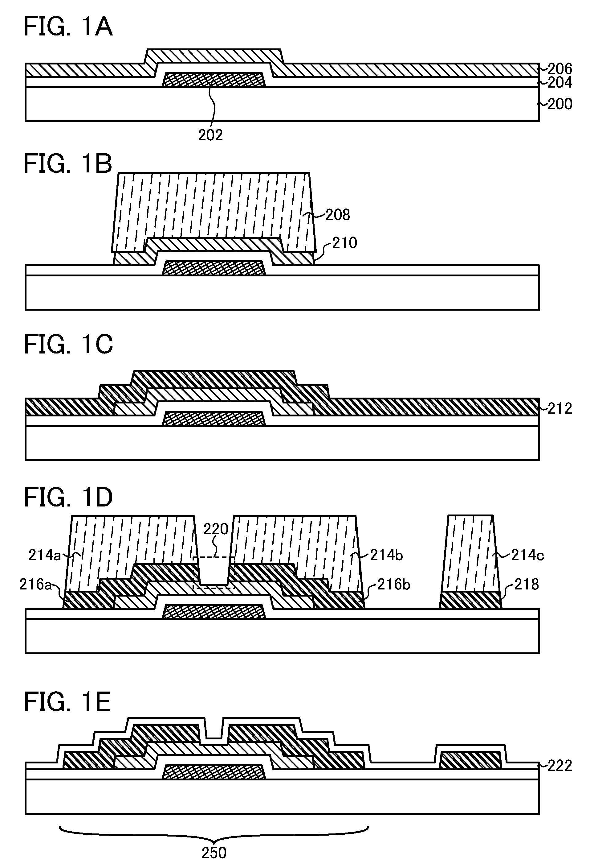
[0059]In this embodiment, an example of a method for manufacturing a semiconductor device is described with reference to FIGS. 1A to 1E.

[0060]First, a gate electrode 202 is formed over a substrate 200 having an insulating surface and then a gate insulating layer 204 and an oxide semiconductor layer 206 are formed over the gate electrode 202 (see FIG. 1A).

[0061]As the substrate 200 having an insulating surface, for example, a glass substrate having a visible light transmitting property, which is used for a liquid crystal display device or the like, can be used. The glass substrate is preferably an alkali-free glass substrate. As an alkali-free glass substrate, for example, a glass material such as aluminosilicate glass, aluminoborosilicate glass, or barium borosilicate glass is used. In addition, as the substrate 200 having an insulating surface, an insulating substrate which is formed of an insulator, such as a ceramic substrate, a quartz substrate, or a sapphire substrate; a semico...

embodiment 2

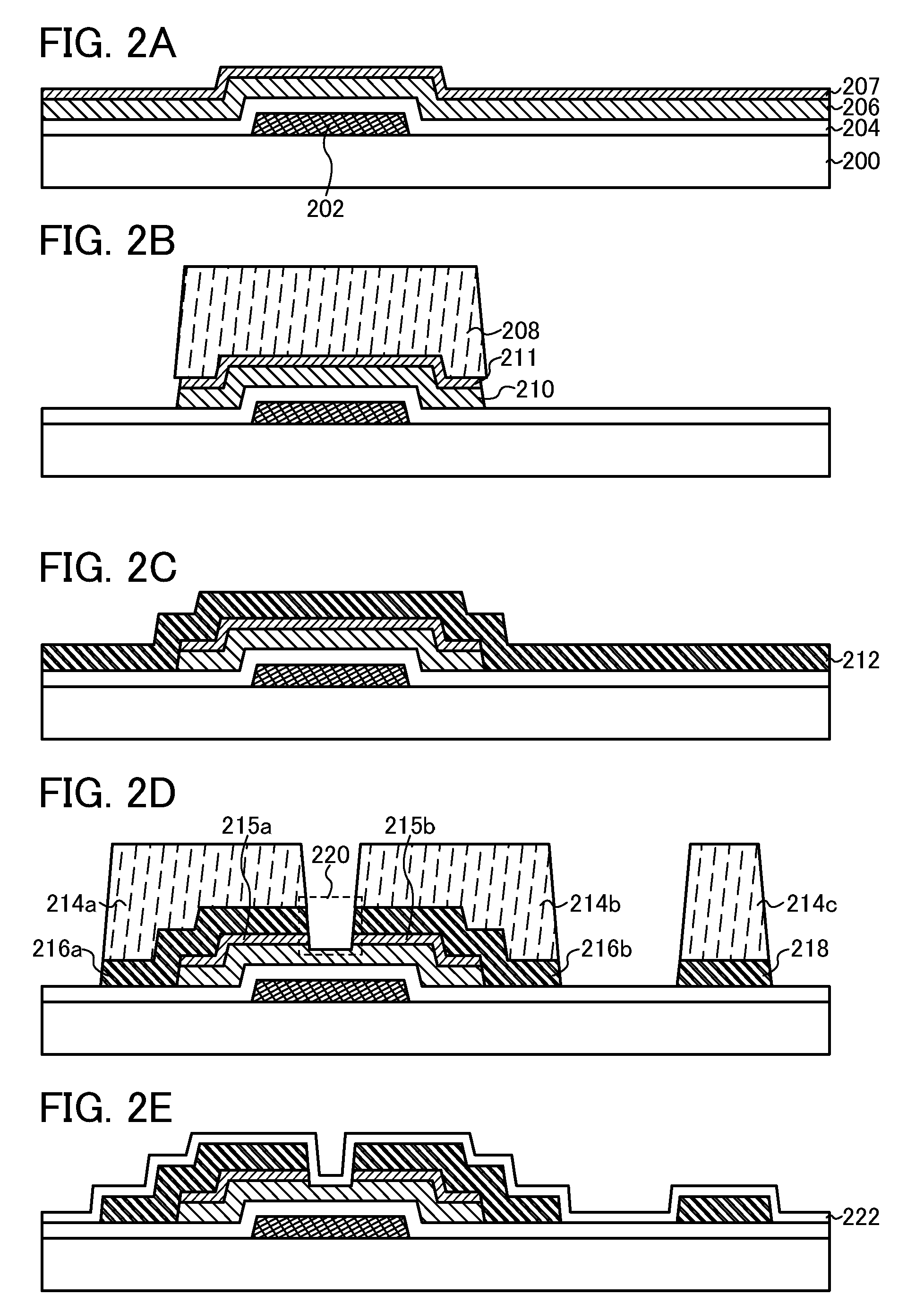
[0092]In this embodiment, a method for manufacturing a semiconductor device, which is different from that of the above embodiment, is described with reference to drawings. Note that many steps of the method for manufacturing a semiconductor device in this embodiment are common to those of Embodiment 1. Therefore, repeated description of the common steps is omitted and description of steps different from that of Embodiment 1 is made below.

[0093]First, a gate electrode 202 is formed over a substrate 200 having an insulating surface and then a gate insulating layer 204 is formed over the gate electrode 202. After that, an oxide semiconductor layer 206 and an oxide semiconductor layer 207 are stacked thereover (see FIG. 2A).

[0094]The materials and manufacturing method of the gate electrode 202, the gate insulating layer 204, and the oxide semiconductor layer 206 can be referred to Embodiment 1.

[0095]The oxide semiconductor layer 207 can be formed using an In—Ga—Zn—O based non-single-cry...

embodiment 3

[0119]In this embodiment, a method for manufacturing a display device which is an example of a usage mode of a semiconductor device is described with reference to drawings. Note that many steps of the manufacturing method described in this embodiment are common to those of Embodiment 1 or Embodiment 2. Therefore, repeated description of the common steps is omitted and description of steps different from that of Embodiment 1 or Embodiment 2 is made below. Note that in the description below, FIGS. 5A to 5C and FIGS. 6A to 6C are cross-sectional views and FIG. 7, FIG. 8, FIG. 9, and FIG. 10 are top views.

[0120]First, wirings and an electrode (a gate wiring including a gate electrode 202, a capacitor wiring 108, and a first terminal 121) are formed over a substrate 200 having an insulating surface (see FIG. 5A and FIG. 7).

[0121]The capacitor wiring 108 and the first terminal 121 can be formed at the same time and using the same material as the gate electrode 202. Note that the material ...


PUM


Abstract

An object is to establish a processing technique in manufacture of a semiconductor device in which an oxide semiconductor is used. A gate electrode is formed over a substrate, a gate insulating layer is formed over the gate electrode, an oxide semiconductor layer is formed over the gate insulating layer, the oxide semiconductor layer is processed by wet etching to form an island-shaped oxide semiconductor layer, a conductive layer is formed to cover the island-shaped oxide semiconductor layer, the conductive layer is processed by dry etching to form a source electrode, and a drain electrode and part of the island-shaped oxide semiconductor layer is removed by dry etching to form a recessed portion in the island-shaped oxide semiconductor layer.

Description

BACKGROUND OF THE INVENTION[0001]1. Field of the Invention[0002]The present invention relates to a method for manufacturing a semiconductor device in which an oxide semiconductor is used.[0003]2. Description of the Related Art[0004]In recent years, a technique for forming a thin film transistor (also referred to as a TFT) using an oxide semiconductor and applying the thin film transistor to an electron device and the like has attracted attention. For example, a technique for forming a switching element of an image display device and the like using zinc oxide or an In—Ga—Zn—O based oxide semiconductor as an oxide semiconductor film is disclosed in Patent Document 1 and Patent Document 2.[0005]Etching treatment is a typical technique for processing an oxide semiconductor (see Patent Document 3 and Patent Document 4); however, there are problem. For example, wet etching is unsuitable for miniaturization of an element since wet etching is isotropic etching. In addition, since a chemical...

Claims


Application Information

Patent Timeline
Patent Type & Authority Applications(United States)
IPC IPC(8): H01L21/465
CPCH01L27/1225H01L29/66969H01L21/465H01L29/7869H01L21/02225H01L21/4763H01L21/67069H01L29/41725H01L29/42312H01L29/4232H10K59/1213H01L27/124G02F1/134309G02F1/136227G09G3/3648G09G3/3677G09G2300/0408G09G2300/0809G09G2310/0251G09G2310/0286G09G2310/08G11C19/28H01L27/127H01L29/78696
Inventor SUZAWA, HIDEOMISASAGAWA, SHINYAMURAOKA, TAIGA
Owner SEMICON ENERGY LAB CO LTD
Why Eureka
Try Eureka