Organic electroluminescence device

Active Publication Date: 2011-05-26
SAMSUNG DISPLAY CO LTD
View PDF12 Cites 2 Cited by
  • Summary
  • Abstract
  • Description
  • Claims
  • Application Information

AI Technical Summary

Benefits of technology

[0021]The organic electroluminescence device with this configuration has the light reflective electrode which is spaced from both the luminescent points by the distances of“d”. This distance of “d” is designed such that the light flux of the light is interfered with the other light flux of the light in order to enhance the light. Or, this distance of “d” is designed such that each one of the light is interfered with the other light in order to enhance the light. Therefore, the light flux or the photon number which enhances the light between the luminescent point and the light reflective ele

Problems solved by technology

However, the patent literature 1 discloses that when the light is reflected by the boundary of the light reflective electrode and the adjacent layer which is adjacent to the light reflective electrode, the phase of the light is shifted by π. Therefore, the phase shift is sufficiently unconsidered by the patent literature 1.
Furthermore, the patent literatures 1 to 3 does not discloses the light scattering region provided to the components such as substrates.
Thus designation causes a thickness reduction between the light emissive

Method used


Image

  • Organic electroluminescence device
  • Organic electroluminescence device
  • Organic electroluminescence device

Examples


example 1

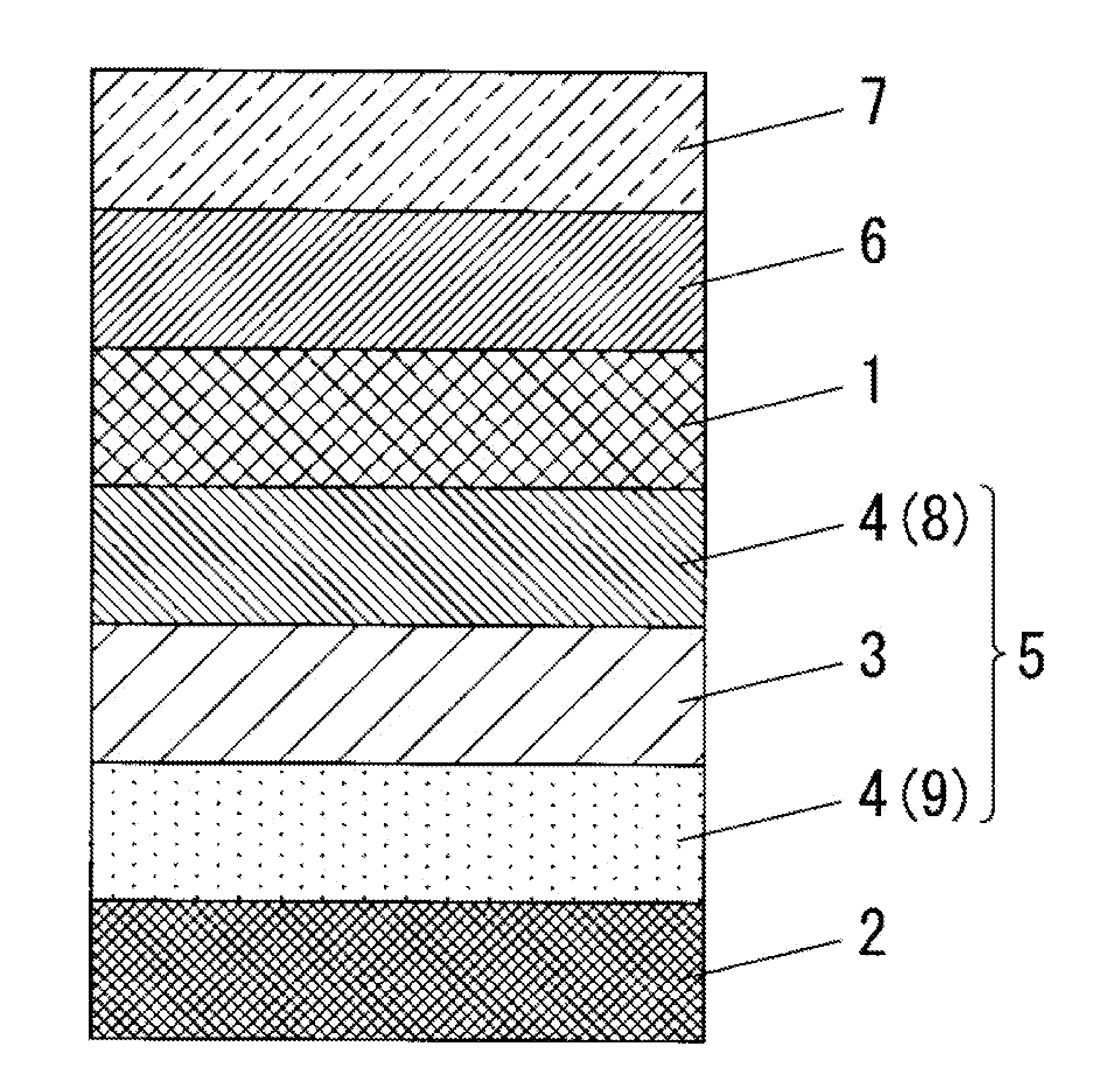
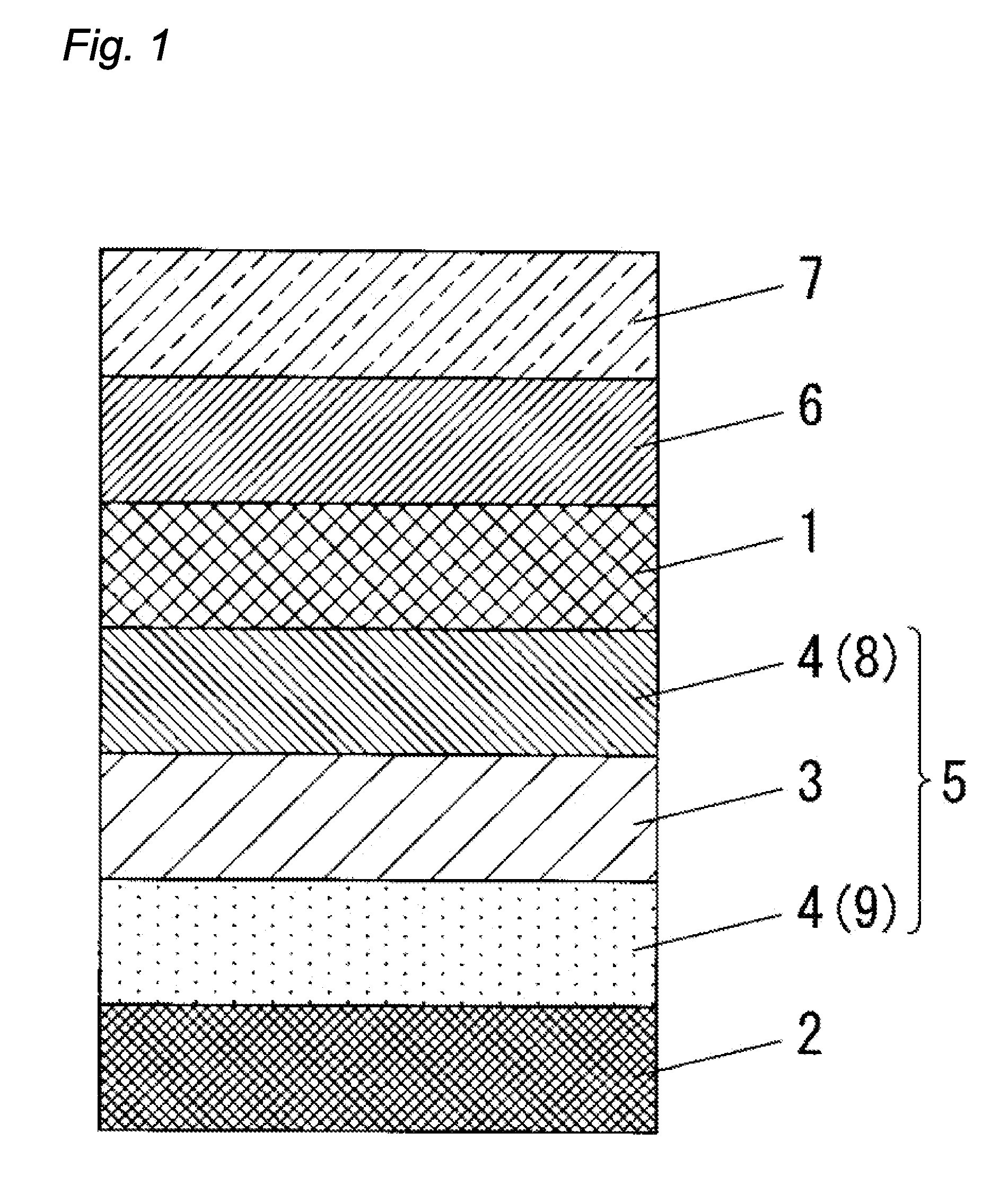
[0058]In the organic electroluminescence device, the glass substrate 6 having a thickness of 0.7 mm was prepared. The glass substrate 6 was provided with ITO film. The ITO film had a thickness of 150 nm and had a sheet resistance of 10 ohm per square. The ITO film had a thickness of 150 nm, and had a sheet resistance of 10 ohm per square. The substrate 6 was etched and cut in order to form the glass substrate 6 with the ITO film having a size shown in FIG. 3. Consequently, the ITO film was formed as the anode which acts as the light transmissive electrode 1. The glass substrate 6 with the ITO was cleaned by ultrasonic cleaning with pure water, acetone, and isopropyl alcohol. Subsequently, the glass substrate 6 with the ITO was cleaned by vapor cleaning with vapor of the isopropyl alcohol. Subsequently, the glass substrate 6 with the ITO was cleaned by UV ozone cleaning for 10 minutes.

[0059]Subsequently, the glass substrate 6 with the ITO was placed within a vacuum deposition equipme...

example 2

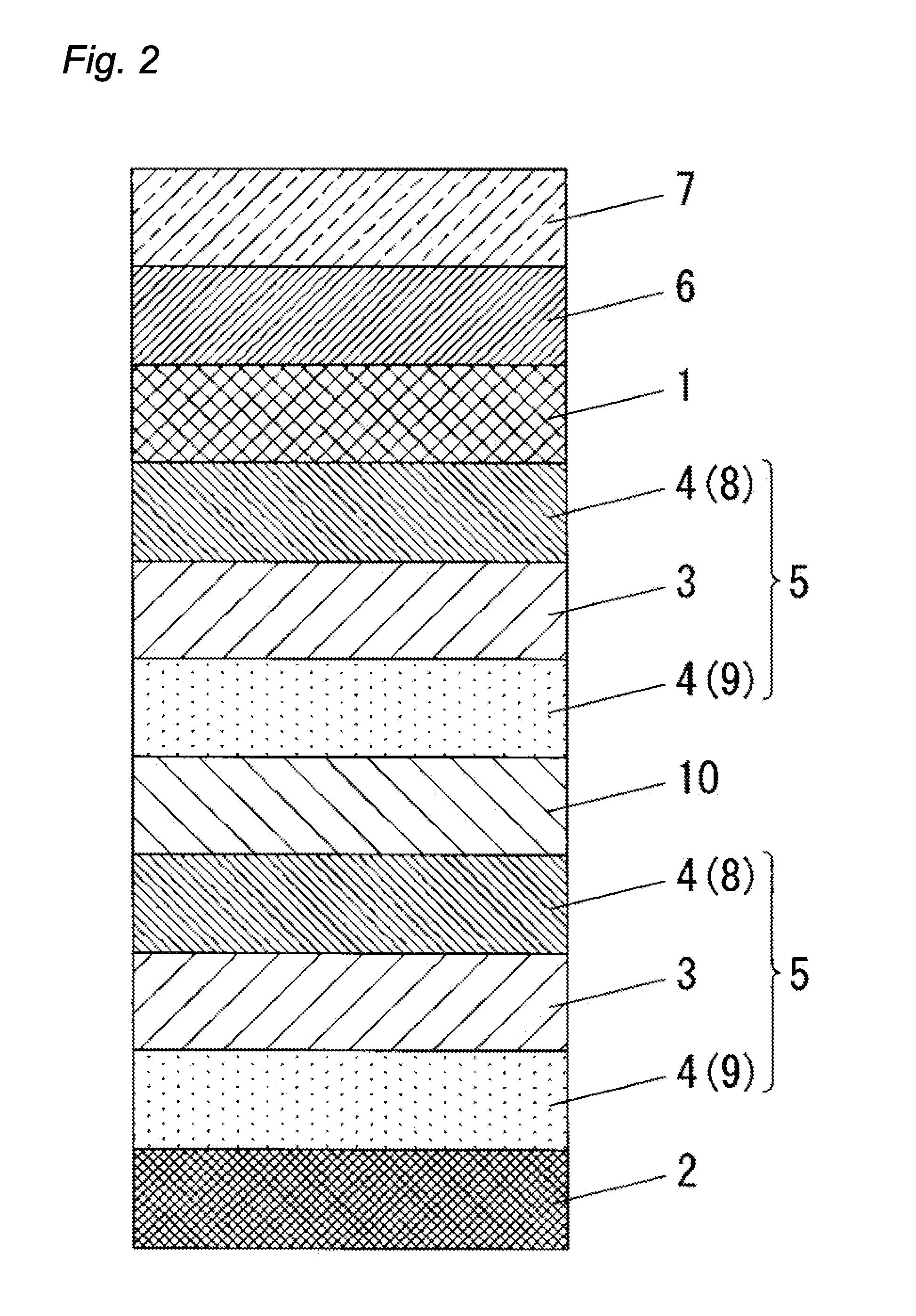
[0060]The organic electroluminescence device was obtained in the same manner as in example 1 except that the electron transport layer 9 had a thickness of 350 nm.

example 3

[0061]The organic electroluminescence device was obtained in the same manner as in example 1 except that the electron transport layer 9 had a thickness of 400 nm.


PUM


Abstract

An organic electroluminescence device comprises a light transmissive substrate, a light scattering region which is disposed on the light transmissive substrate, and a light emissive layer having a luminescent point. The luminescent point is spaced from the light reflective electrode by a distance of d which satisfies the following equation:
nd=a×λ4(2+φπ)whereinφ=tan-1{2(n1k2-n2k1)n12-n22+k12-k22}.
    • λ is a wavelength of a specific light emitted from said light emissive layer.
    • n is a refractive index of a layer disposed between the luminescent point of the light emissive layer and the light reflective electrode, with respect to the wavelength of λ.
    • n1 and k1 are respectively a refractive index and an attenuation coefficient of the layer disposed between the luminescent point of the light emissive layer and the light reflective electrode, and is in contact with said light reflective electrode, with respect to the wavelength of λ.
    • n2 and k2 are respectively a refractive index and an attenuation coefficient of the light reflective electrode, with respect to the wavelength of λ.
    • a is a value that satisfies a relation of “1.28<a≦−5.56×norg/nEML+7.74”
    • norg is a refractive index of the layer disposed which is located between the luminescent point of the light emissive layer and the light reflective electrode and which is in contact with the light emissive layer, with respect to the wavelength of λ.
    • nEML is a refractive index of the light emissive layer with respect to the wavelength of λ.

Description

TECHNICAL FIELD[0001]This invention relates to organic electroluminescence devices which are used for illumination light sources, backlights of the liquid crystal display instrument, and flat panel displays. Particularly, this invention relates to an organic electroluminescence devices having good luminescence properties by employing a suitable optical design.BACKGROUND ART[0002]The organic electroluminescence device comprises a substrate, a light transmissive electrode which acts as an anode, a hole transport layer, a light emissive layer, an electron transport layer, and a light reflective electrode which acts as a cathod. The light transmissive electrode, the hole transport layer, the light emissive layer, the electron transport layer, and the light reflective electrode are formed on the substrate in order. When the voltage is applied between the light transmissive electrode and the light reflective electrode, electrons are injected into the light emissive layer through the elect...

Claims


Application Information

Patent Timeline
IPC IPC(8): H01L51/44
CPCH01L51/0052H01L51/0059H01L51/0067H01L2251/558H01L51/0073H01L51/0079H01L51/5265H01L51/007H10K85/6565H10K85/321H10K85/615H10K85/631H10K85/654H10K85/6574H10K50/852H10K2102/351Y02B20/30H10K50/818H10K2102/301
Inventor IDE, NOBUHIROYAMANA, MASAHITOTSUJI, HIROYAITO, NORIHIROMITSUTAKE, YOSHIONAKAMURA, MASAHIROYAMAKI, TAKEYUKI
Owner SAMSUNG DISPLAY CO LTD
Why Eureka
Try Eureka