Array substrate for liquid crystal display device and method of fabricating the same

Active Publication Date: 2011-06-02
LG DISPLAY CO LTD
View PDF4 Cites 11 Cited by
  • Summary
  • Abstract
  • Description
  • Claims
  • Application Information

AI Technical Summary

Benefits of technology

[0026]An object of the present invention is to provide an array substrate having an advantage in production costs.
[0027]Another object of the present invention is to provide an array substrate being

Problems solved by technology

As a number of the mask process is increased, production costs are increase and production yield is decreased.
Unfortunately, there a

Method used


Image

  • Array substrate for liquid crystal display device and method of fabricating the same
  • Array substrate for liquid crystal display device and method of fabricating the same
  • Array substrate for liquid crystal display device and method of fabricating the same

Examples


Example

[0038]Reference will now be made in detail to the preferred embodiments, examples of which are illustrated in the accompanying drawings.

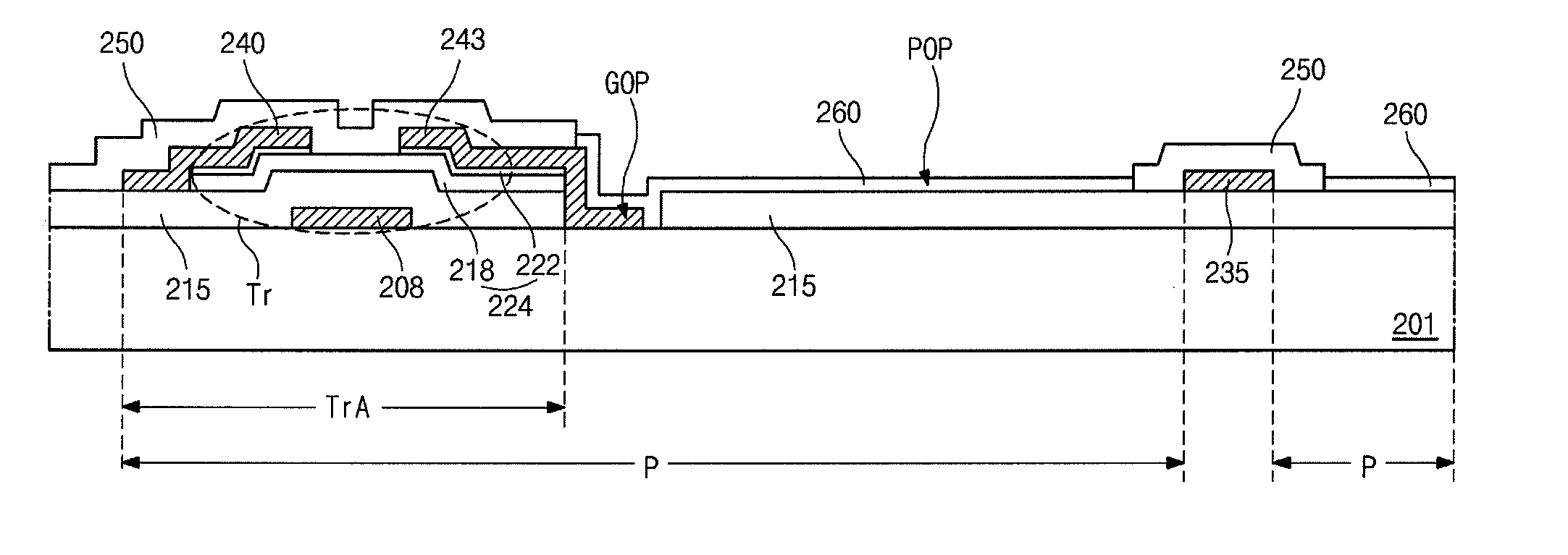
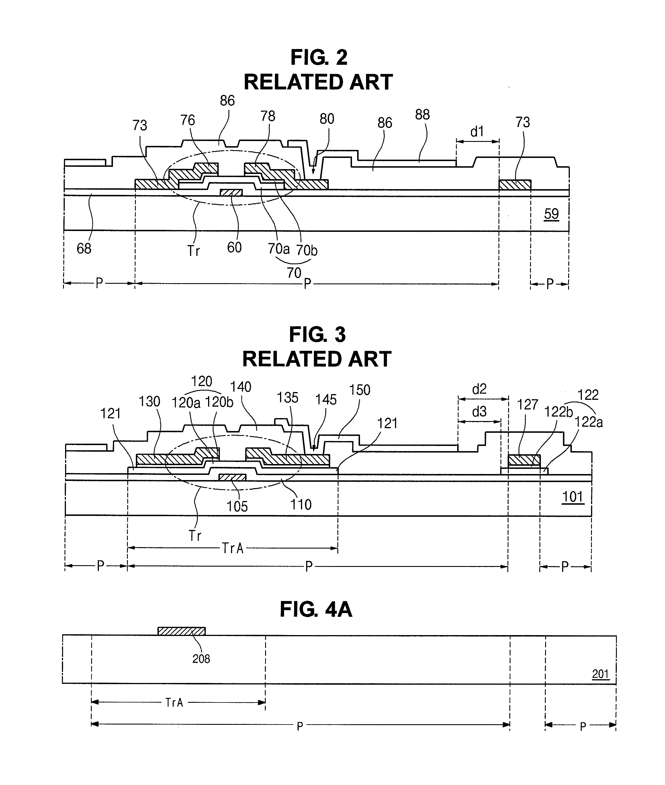
[0039]FIGS. 4A to 4M are cross-sectional views showing a fabricating process of an array substrate according to the present invention. A region, where a thin film transistor (TFT) is formed, is defined as a switching region TrA in a pixel region P.

[0040]FIG. 4A shows a first mask process. In FIG. 4A, a first metallic material layer (not shown) is formed on the substrate 201. The substrate 201 is transparent and has an insulating property. The first metallic material layer is patterned by a first mask process to form the gate line (not shown) and the gate electrode 208. The gate electrode 208 is connected to the gate line and is disposed in the switching region TrA. Although not shown, the first mask process includes a step of forming a photoresist (PR) layer, a step of exposing the PR layer to light using a first mask, a step of developing the expos...


PUM


Abstract

An array substrate for a liquid crystal display device includes a gate line on a substrate; a gate electrode connected to the gate line; a gate insulating layer on the gate line and the gate electrode and including a gate opening; an active layer on the gate insulating layer and overlapping the gate electrode; an ohmic contact layer on the active layer; a source electrode on the ohmic contact layer; a drain electrode on the ohmic contact layer and spaced apart from the source electrode, wherein one end of the drain electrode is disposed in the gate opening; a data line on the gate insulating layer and connected to the source electrode, the data line crossing the gate line; a passivation layer on the data line and the source and drain electrodes and including a pixel opening, wherein the pixel opening exposes the drain electrode in the gate opening and a portion of the gate insulating layer; and a pixel electrode on the gate insulating layer and in the pixel opening, the pixel electrode contacting the one end of the drain electrode in the gate opening.

Description

[0001]The present application claims the benefit of Korean Patent Application No. 10-2009-0118281 filed in Korea on Dec. 2, 2009, which is hereby incorporated by reference.BACKGROUND OF THE INVENTION[0002]1. Field of the Invention[0003]The present invention relates to a liquid crystal display (LCD) device and more particularly to an array substrate including a thin film transistor having improved properties and a method of fabricating the array substrate.[0004]2. Discussion of the Related Art[0005]Since a liquid crystal display (LCD) device has characteristics of light weight, thinness and low power consumption, LCD devices have been widely used. Among the known types of LCD devices, active matrix LCD (AM-LCD) devices, which have thin film transistors (TFTs) arranged in a matrix form, are the subject of significant research and development because of their high resolution and superior ability in displaying moving images.[0006]Generally, the LCD device is manufactured through an arra...

Claims


Application Information

Patent Timeline
IPC IPC(8): H01L33/08H01L33/00
CPCH01L27/124H01L27/1288G02F1/136
Inventor AHN, SUNG-HOONLIM, KYOUNG-NAMKIM, HWAN
Owner LG DISPLAY CO LTD
Why Eureka
Try Eureka