

High Performance Low Power Output Drivers
a low-power output and driver technology, applied in the field of output drivers, can solve the problems of limiting the support of cmos drivers for high-performance interfaces, power consumption of conventional sai drivers, and the inability to meet the requirements of high-performance systems, so as to reduce power consumption, consume less power, and consume less power
- Summary
- Abstract
- Description
- Claims
- Application Information
AI Technical Summary
Benefits of technology
Problems solved by technology
Method used
Image

Examples
Embodiment Construction
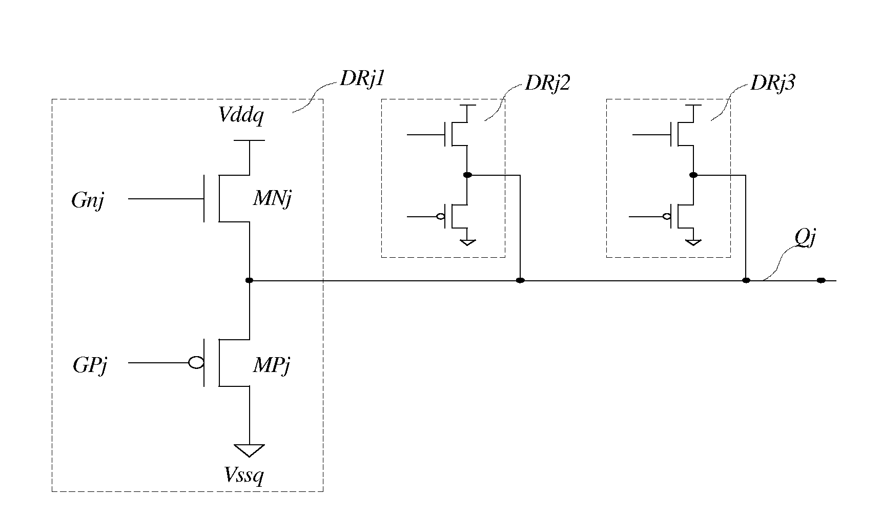
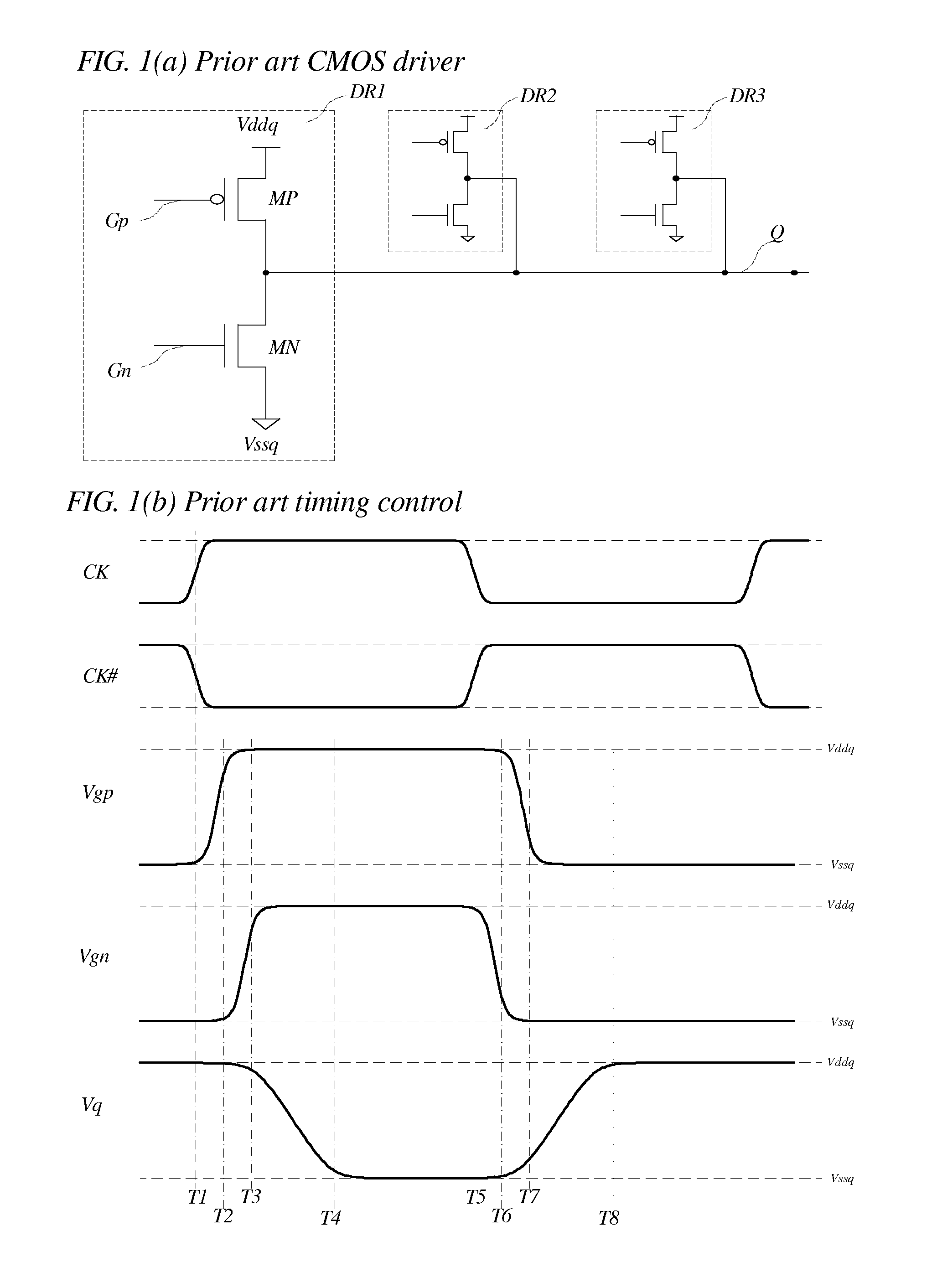
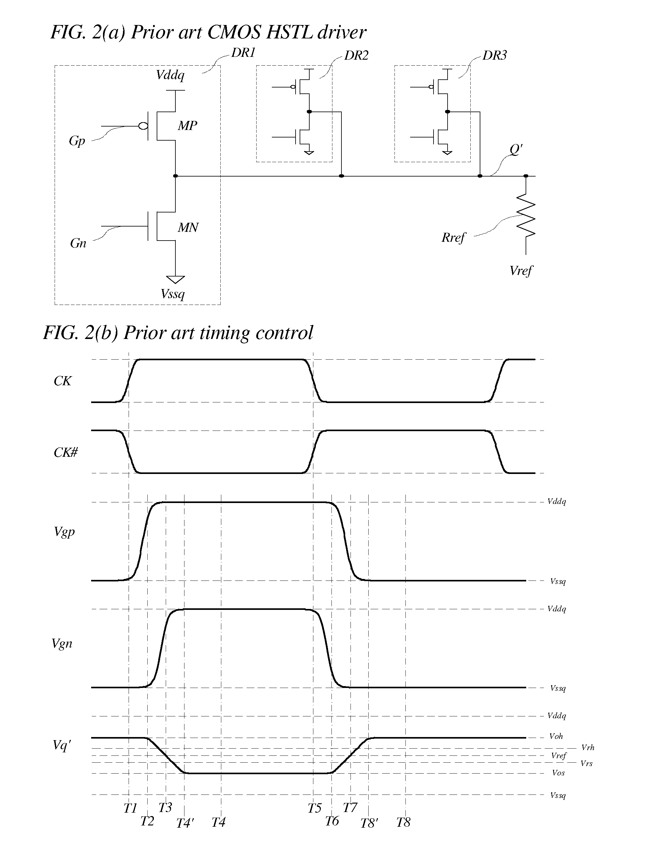
[0013]One of the primary objectives of the preferred embodiments is, therefore, to provide output drivers that reduce power consumption at quiescent state. Another primary objective of the preferred embodiments is to provide output drivers that can switch between multiple levels of high accuracy output voltages while consuming less power. Another objective is to support small amplitude interface protocols without using termination resistors. Another objective is to provide termination circuits working with output drivers of the present invention to consume less power. Another objective is to reduce the cost of output drivers that drive memory interfaces such as HSTL or SSTL interfaces. Another objective is to improve the fan out of partial voltage output drivers. These and other objectives are achieved by using output drivers comprising n-channel pull up transistors and / or p-channel pull down transistors biased with proper gate voltages, and / or using RC termination circuits.
[0014]Wh...
PUM
 Abstract
Description
Claims
Application Information