Multi-directional resonant-type electromagnetic wave absorber, method for adjusting electromagnetic wave absorption performance using the same and manufacturing method of the same

a technology of electromagnetic waves and absorbers, applied in the direction of electrical devices, coatings, antennas, etc., can solve the problems of confusion of brain waves, lowering eyesight, and the influence of electromagnetic waves generated from terminals on the human body, and achieves the effect of easy manufacturing and easy adjustment of electromagnetic absorption characteristics

Inactive Publication Date: 2011-06-09
ELECTRONICS & TELECOMM RES INST
View PDF4 Cites 20 Cited by
  • Summary
  • Abstract
  • Description
  • Claims
  • Application Information

AI Technical Summary

Benefits of technology

[0011]Further, the present invention provides a multi-directional electromagnetic wave absorber, which is easy to manufacture, enables the adjustment of thickness, and makes it easy to adjust electromagnetic absorption characteristics of different frequency bands through the adjustment of design parameters by using an electromagnetic bandgap structure and a resistive material.

Problems solved by technology

However, as these portable devices have been increasingly used, the influence of electromagnetic waves generated from the terminals on the human body becomes an important issue.
The influence of electromagnetic waves at a frequency band used by portable terminals on the human body is not yet clearly found, but it has been reported that the electromagnetic waves may cause various diseases such as leukemia, a brain tumor, a headache, a lowering of eyesight, and when they are accumulated in the human body, confusion of brain waves, destruction of men's reproductive function, and the like.
Moreover, cases of malfunctions between information communication devices caused by undesired electromagnetic waves are steadily being reported, and steady research on EMI / EMC problems is under way across the world.
Since such electromagnetic wave absorbers are generally developed after much trial and error, it is disadvantageous in that the manufacturing process thereof is complicated and it is highly difficult to adjust an absorption frequency band and absorption characteristics.
However, such a Salisbury screen is disadvantageous in that the thickness of the dielectric spacer from the metal conductive ground plane must be more than at least λ / 4.
However, this structure has the limitation that only electromagnetic waves in one direction can be absorbed.

Method used


Image

  • Multi-directional resonant-type electromagnetic wave absorber, method for adjusting electromagnetic wave absorption performance using the same and manufacturing method of the same
  • Multi-directional resonant-type electromagnetic wave absorber, method for adjusting electromagnetic wave absorption performance using the same and manufacturing method of the same
  • Multi-directional resonant-type electromagnetic wave absorber, method for adjusting electromagnetic wave absorption performance using the same and manufacturing method of the same

Examples


first embodiment

[0076]FIG. 10 is a flowchart showing a manufacturing method of a resonant-type electromagnetic wave absorber.

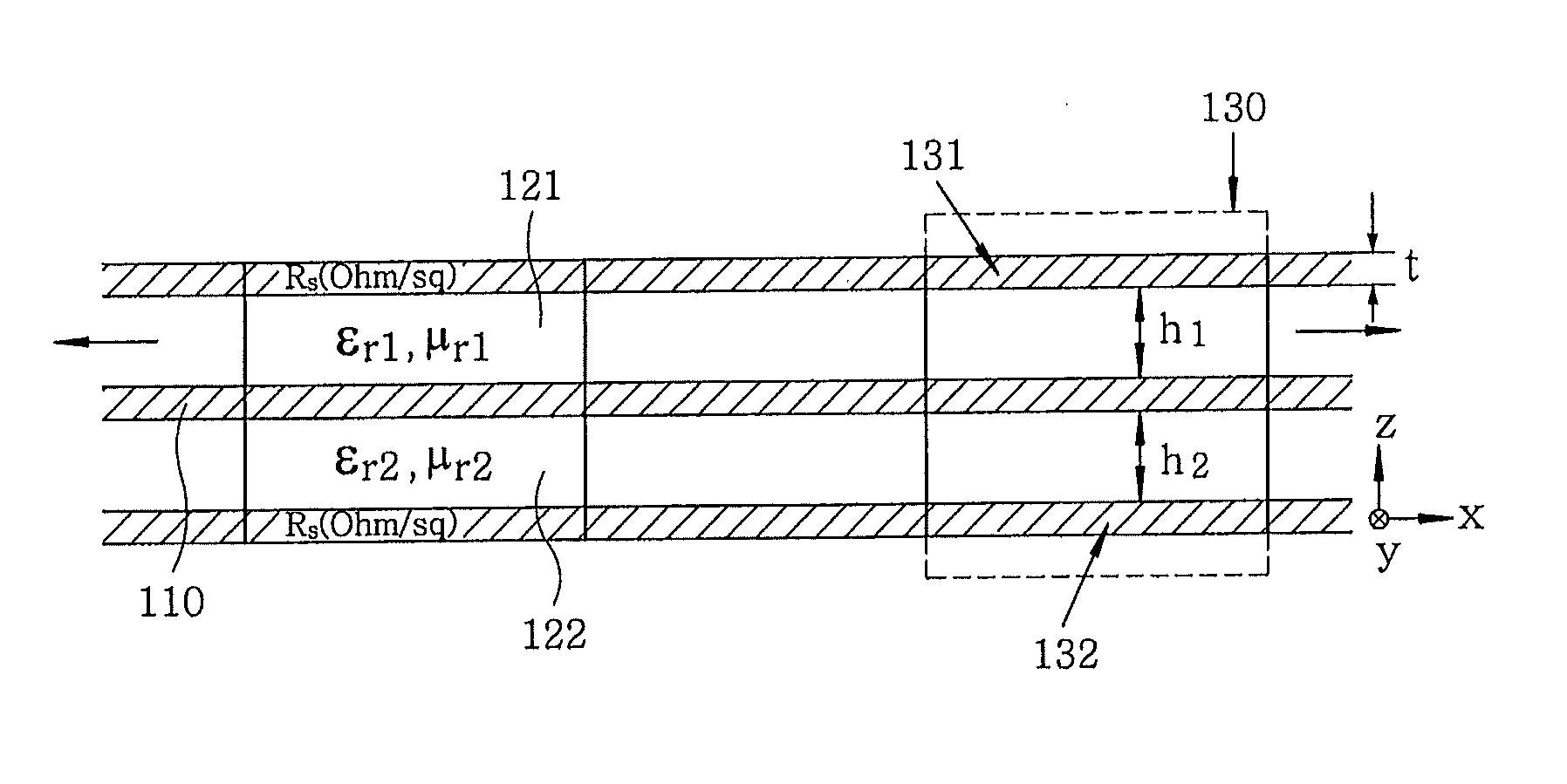
[0077]Referring to FIG. 10, first, a first dielectric layer 121 is formed in step S100. A thickness, permittivity, and permeability of the first dielectric layer 121 may be determined based on desired electromagnetic absorption characteristics.

[0078]Second, at least one ground layer 110 is formed on top of the first dielectric layer 121 in step S200. The ground layer 110 may be formed of a metal conductive material, and the number of the ground layer 110, the reflection coefficient thereof, and the like may be determined based on desired electromagnetic absorption characteristics.

[0079]Third, a second dielectric layer 122 is formed on top of the ground layer 110 in step S300. A thickness, permittivity, and permeability of the second dielectric layer 122 may be determined based on desired electromagnetic absorption characteristics.

[0080]Fourth, a first resistive pattern layer ...

second embodiment

[0083]FIG. 11 is a flowchart showing a manufacturing method of a resonant-type electromagnetic wave absorber in accordance with the present invention.

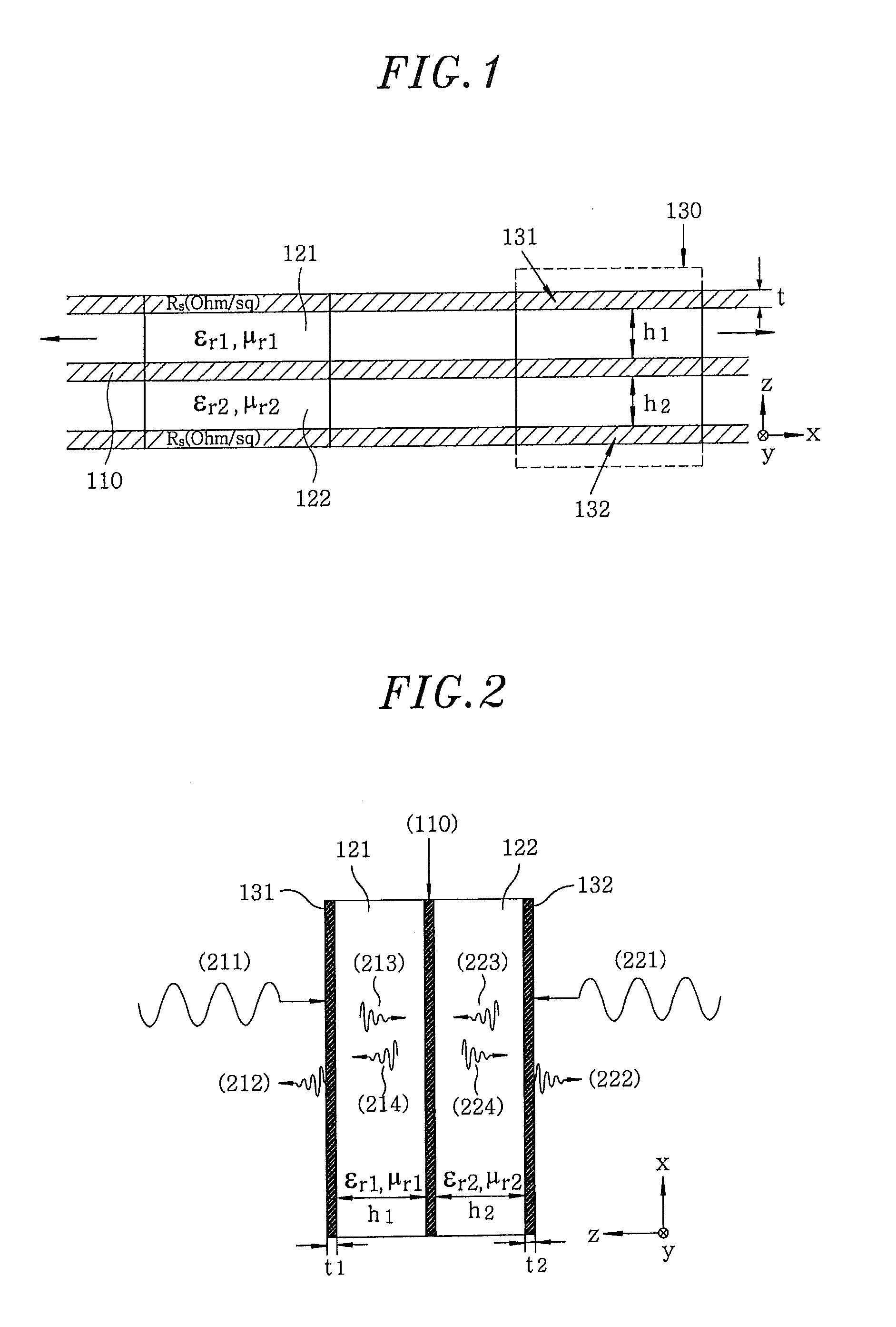
[0084]Referring to FIG. 11, a ground layer 110 is formed in step S150. After that, a first dielectric layer 121 is formed on top of the ground layer 110 in step S250, and then a second dielectric layer 122 is formed under the ground layer 110 in step S350. Next, a first resistive pattern layer 131 is formed on an outer surface of the first dielectric layer 121 in step S450, and a second resistive pattern layer 132 is formed on an outer surface of the second dielectric layer 122 in step S550. A detailed process of the manufacturing method of the second embodiment may be performed in the same way as that of the manufacturing method of the first embodiment.

[0085]In accordance with the present invention, electromagnetic waves incident in various directions can be simultaneously absorbed by using a multi-directional electromagnetic wave abs...


PUM


Abstract

A multi-directional resonant-type electromagnetic wave absorber includes: at least one ground layer; a first dielectric layer and a second dielectric layer respectively formed on different outer surfaces of the ground layer; a first resistive pattern layer formed on an outer surface of the first dielectric layer; and a second resistive pattern layer formed on an outer surface of the second dielectric layer. Herein, the electromagnetic absorption performance is adjusted by changing one or more of thicknesses, permittivities, and permeabilities of the dielectric layers, thicknesses of the resistive pattern layers, and a reflection coefficient of the ground layer.

Description

CROSS-REFERENCE(S) TO RELATED APPLICATION(S)[0001]The present invention claims priority of Korean Patent Application No. 10-2009-0120443, filed on Dec. 7, 2009, which is incorporated herein by reference.FIELD OF THE INVENTION[0002]The present invention relates to a multi-directional resonant-type electromagnetic wave absorber, a method for adjusting electromagnetic wave absorption performance using the same, and a manufacturing method of the same; and, more particularly, to a multi-directional resonant-type electromagnetic wave absorber made of a resistive material, which can absorb electromagnetic waves in a desired frequency band by using an alignment structure composed of a periodic array of a unit cell pattern of an electromagnetic bandgap, a method for adjusting electromagnetic wave absorption performance using the same, and a manufacturing method of the same.BACKGROUND OF THE INVENTION[0003]As information technology (IT) has been rapidly developed and a human's desire for comm...

Claims


Application Information

Patent Timeline
Patent Type & Authority Applications(United States)
IPC IPC(8): H01Q17/00B05D5/12
CPCH01Q17/007H01Q17/00H05K9/00
Inventor SIM, DONG-UK
Owner ELECTRONICS & TELECOMM RES INST
Why Eureka
Try Eureka