Active Dual in Line Memory Module Connector with Re-driven Propagated Signals

a dual-in-line memory module and propagation signal technology, which is applied in the direction of fixed connections, coupling device connections, printed circuit aspects, etc., can solve the problems of reflection of signals, degrade signal quality, and none of the prior art connectors used in the industry have ever accommodated active circuits, etc., to facilitate high-density memory module system operation

Active Publication Date: 2011-06-16
CALLAHAN CELLULAR L L C
View PDF8 Cites 17 Cited by
  • Summary
  • Abstract
  • Description
  • Claims
  • Application Information

AI Technical Summary

Benefits of technology

[0018]It is the object of the present invention to provide an active connector which facilitates high density memory module systems operating at high frequency data rates.
[0020]In accordance with a second aspect of the invention, the connector consists of two rigid double faced PCB, single or multiple layers, having long and short edges on the perimeter separated by material of thickness sufficient to form a cavity between the two PCBs, and to maintain alignment and rigidity of the PCB sides.
[0022]In accordance with a fourth aspect of the invention, the rectangular PCB pieces are attached to material which serves to keep the two PCB pieces in a parallel arrangement, thus creating a physical cavity for DIMM acceptance. This arrangement provides support and attachment of two latching mechanisms, one on each end in line with the cavity, for securing the inserted DIMM in position and for assisting in the extraction of the DIMM from the cavity. It further provides guiding pins for alignment of the connector on the proper position on the motherboard at time of solder reflow.

Problems solved by technology

None of those prior art connectors used in the industry have ever accommodated active circuits as an integral part of the physical structure.
Said formed pins are farther away from ground or VCC pins and as such present an impedance alteration and discontinuity which causes reflections of the signals.
In addition, reflection from each DIMM load degrades the quality of the signal.
However, such an arrangement of DIMMs and memory chips slows down the data rate.
The number of connectors on a motherboard of prior-art systems is constantly shrinking for space availability, frequency requirements, heat considerations and costs.
However, the ever increasing demand for more memory capacity requires techniques to allow more memory capacity in restricted numbers of connectors with ability to provide heat dissipation.
However, in the memory sub-system of prior art designs such solution has been impractical and requires more space on the motherboard, thus increasing the cost and complexity of the system.
Another inhibiting factor is the long propagation delay due to the lengths of the repeater transmission lines in a multi-DIMM system on the motherboard.
Yet another factor is the presence of long connecting stubs that create signal reflections, thus further distorting the quality of the signal.
Bad signal quality results in receiver data bit errors.

Method used


Image

  • Active Dual in Line Memory Module Connector with Re-driven Propagated Signals
  • Active Dual in Line Memory Module Connector with Re-driven Propagated Signals
  • Active Dual in Line Memory Module Connector with Re-driven Propagated Signals

Examples


Embodiment Construction

[0050]The invention is better explained by reference to the drawings described above, and to the detailed descriptions and explanations which follow.

DEFINITIONS

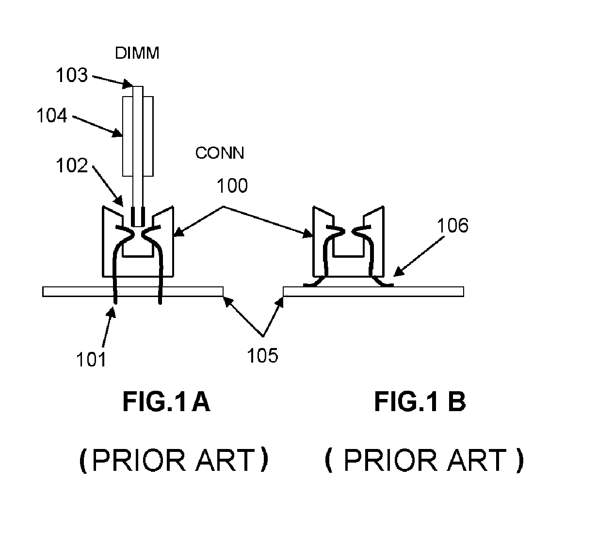
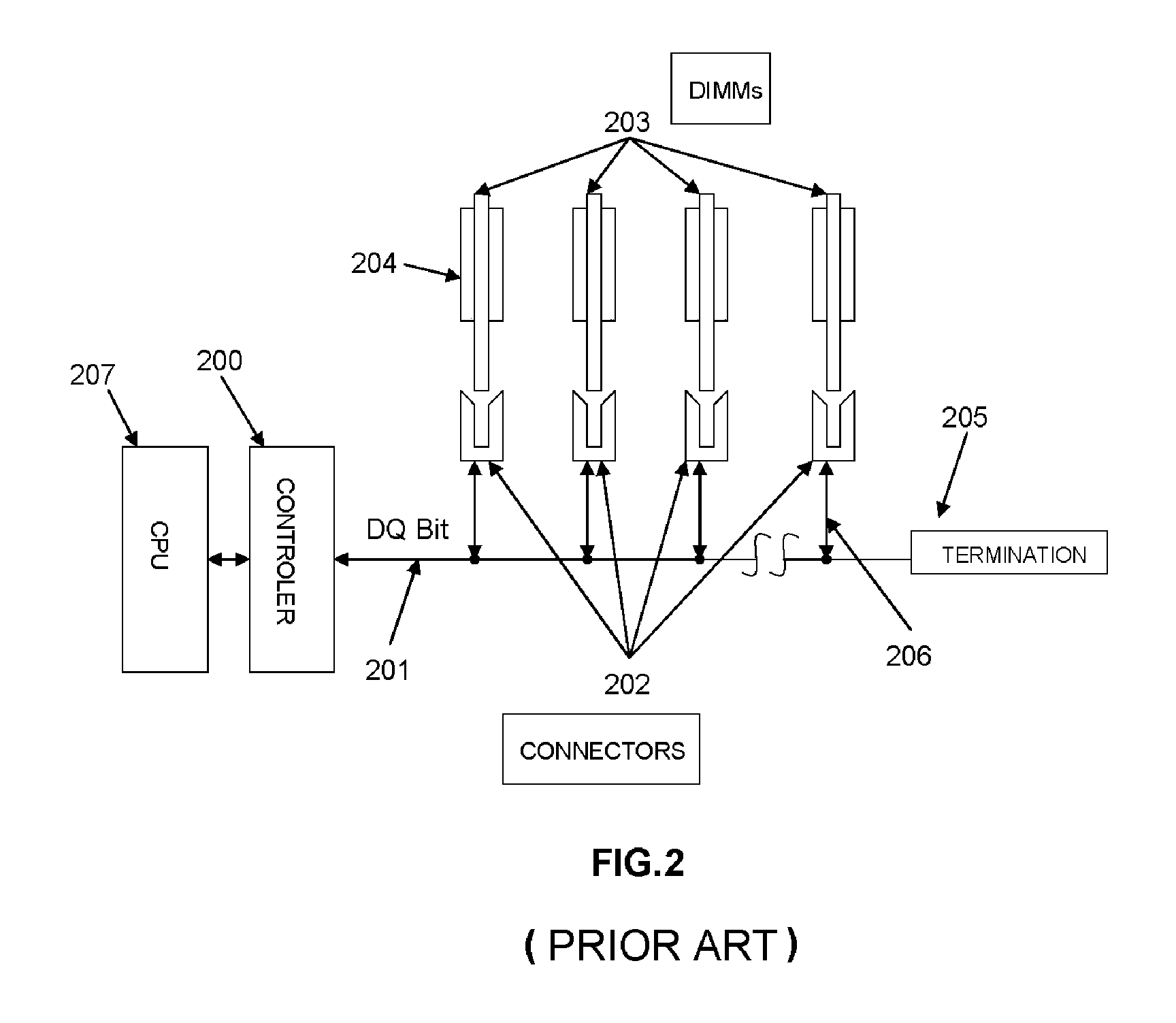
[0051]The term “PCB” will be used to describe printed circuit board assemblies, which contain conducting materials including wiring leads, pads, and other features affixed to the surface, usually by a process of etching. Unless otherwise specified, PCBs are assumed to be rigid.

[0052]The term “Flex PCB” will be used to describe printed circuit board assemblies which are flexible.

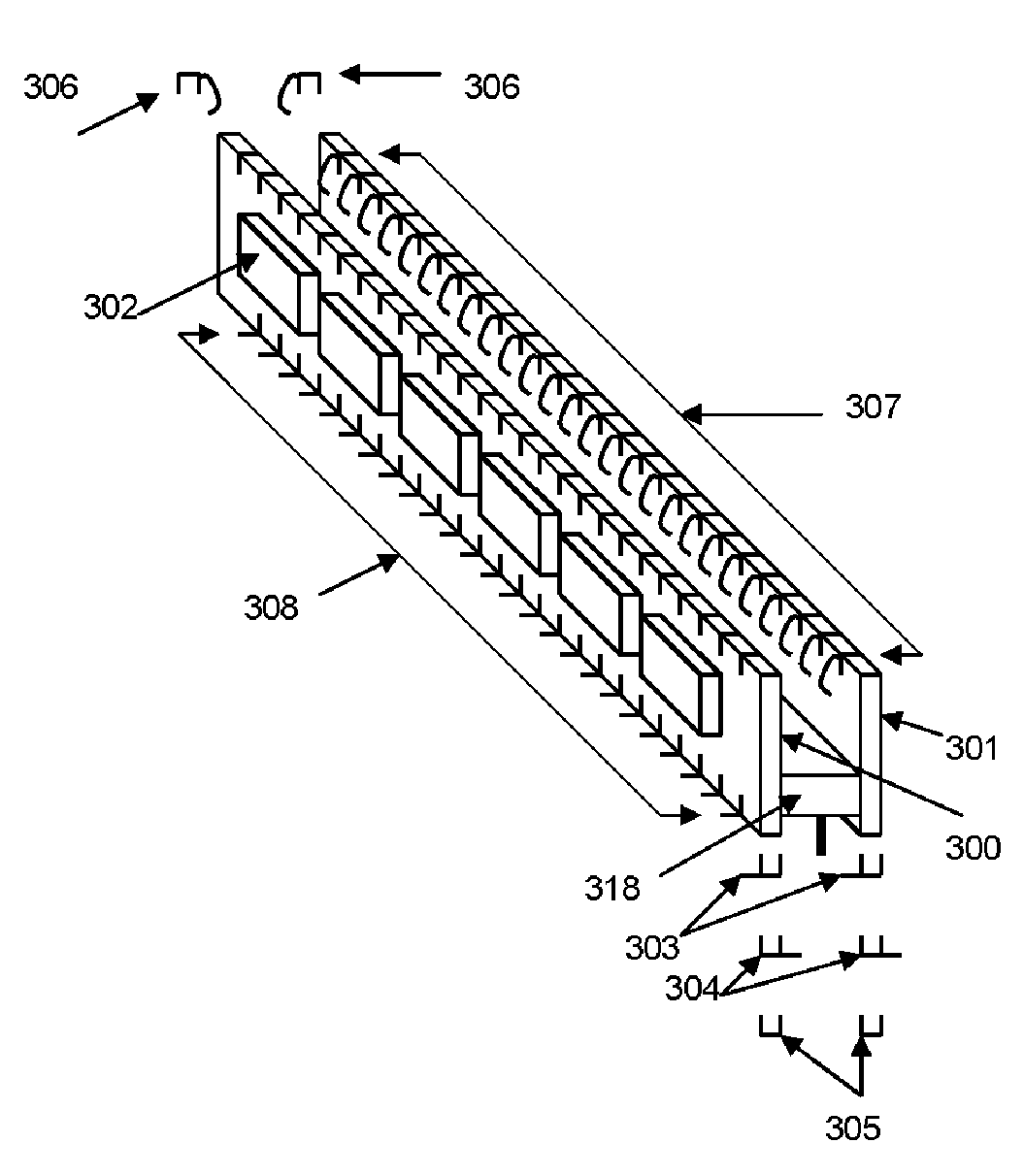
[0053]The term “re-driver chip” will be used to describe the integrated circuit chip, located on the connector of the present invention or in close proximity to it, which contains both receivers and drivers that process data signals of the memory modules, in addition to other circuitry to support these functions. The re-driver chip in an alternative embodiment may also contain circuits that perform addressing and command and control functions.

[0054]The...


PUM


Abstract

An Active edge connector for memory modules has a base including two PCB sides and a spacer separating the sides, with driver chips mounted on each side of each side, printed wiring electrically connecting a first set of electrical signals from each of the driver chips to a mother board on which the connector is mounted, and printed wiring for electrically connecting a second set of electrical signals from each of the driver chips to a memory module inserted in the edge connector. When a group of connectors are mounted on a mother board, electrical signals arriving at the first connector are routed to its driver chips, producing re-driven signals to the next connector, and so on. A decoder circuit provides addressing signals determining the last such connector to which the signals are intended, and which prevents the signals from going to any connectors containing memories not addressed.

Description

[0001]This application claims priority based on U.S. patent application Ser. No. 11 / 831,062 filed on Jul. 31, 2007 for “Active Dual in Line Memory Module Connector with Re-driven Propagated Signals,” as well as Provisional Patent 60 / 834,844 (Aug. 2, 2006), for “Active dual in line memory module connector (ADIMMC) with re-driven propagated signals”.FIELD OF THE INVENTION[0002]This invention relates to the field of systems and methods for creating high capacity Dual In-Line Memory Module (DIMM) connectors with controlled impedance. Said connectors accommodate active circuits to meet requirements of high density memory module systems operating at high frequency data rates. Structures containing the proposed DIMM systems provide point to point connections in a series signal propagation arrangement.DESCRIPTION RELATIVE TO THE PRIOR ART[0003]Throughout the evolution of the computer memory systems, memory chips have either been used soldered on the motherboard or have been packaged in smal...

Claims


Application Information

Patent Timeline
Patent Type & Authority Applications(United States)
IPC IPC(8): H01R13/66H01R13/00
CPCH01R12/62H01R12/721H01R13/6473H01R13/6658H05K1/141H05K1/147H05K2201/10386H05K3/366H05K2201/045H05K2201/049H05K2201/056H05K2201/10159H05K2201/10325H05K1/189
Inventor KARABATSOS, CHRIS
Owner CALLAHAN CELLULAR L L C
Why Eureka
Try Eureka