Remote Doped High Performance Transistor Having Improved Subthreshold Characteristics

a high-performance, transistor technology, applied in the direction of semiconductor devices, semiconductor/solid-state device details, electrical apparatus, etc., can solve the problems of less mobility, difficult control of short channel effects, and unsuitable semiconductor structures and materials, so as to improve the short channel characteristics of the transistor, and the effect of undoping the channel

Inactive Publication Date: 2011-06-23
INTEL AMERICAS INC +1
View PDF5 Cites 2 Cited by
  • Summary
  • Abstract
  • Description
  • Claims
  • Application Information

AI Technical Summary

Benefits of technology

[0005]The present disclosure provides for an apparatus, system, and method which enables the advantages of both the high mobility of undoped channels, and the better short channel characteristics of doped channels by the use of a remote doped layer. In one embodiment, a Field-Effect Transistor (FET) is provided which includes a channel layer configured to convey charge between a source portion and a drain portion of the FET, when the FET is in an active state. Further, the FET may include a barrier layer adjacent to the channel layer. The barrier layer may comprise...

Problems solved by technology

Unfortunately, certain semiconductor structures and materials may become unsuitable as the size decreases.
More specifically in transistor design, with the reduction of channel length it is more difficult to control short channel effects.
However, such doping eventually increases scattering, which leads to lower mobility and, thus, frustrates the main advantage of high mobility channel materials.
Doped channels also come with other drawbacks such as variabilit...

Method used


Image

  • Remote Doped High Performance Transistor Having Improved Subthreshold Characteristics
  • Remote Doped High Performance Transistor Having Improved Subthreshold Characteristics
  • Remote Doped High Performance Transistor Having Improved Subthreshold Characteristics

Examples


Embodiment Construction

[0020]Various features and advantageous details are explained more fully with reference to the nonlimiting embodiments that are illustrated in the accompanying drawings and detailed in the following description. Descriptions of well known starting materials, processing techniques, components, and equipment are omitted so as not to unnecessarily obscure the invention in detail. It should be understood, however, that the detailed description and the specific examples, while indicating embodiments of the invention, are given by way of illustration only, and not by way of limitation. Various substitutions, modifications, additions, and / or rearrangements within the spirit and / or scope of the underlying inventive concept will become apparent to those skilled in the art from this disclosure.

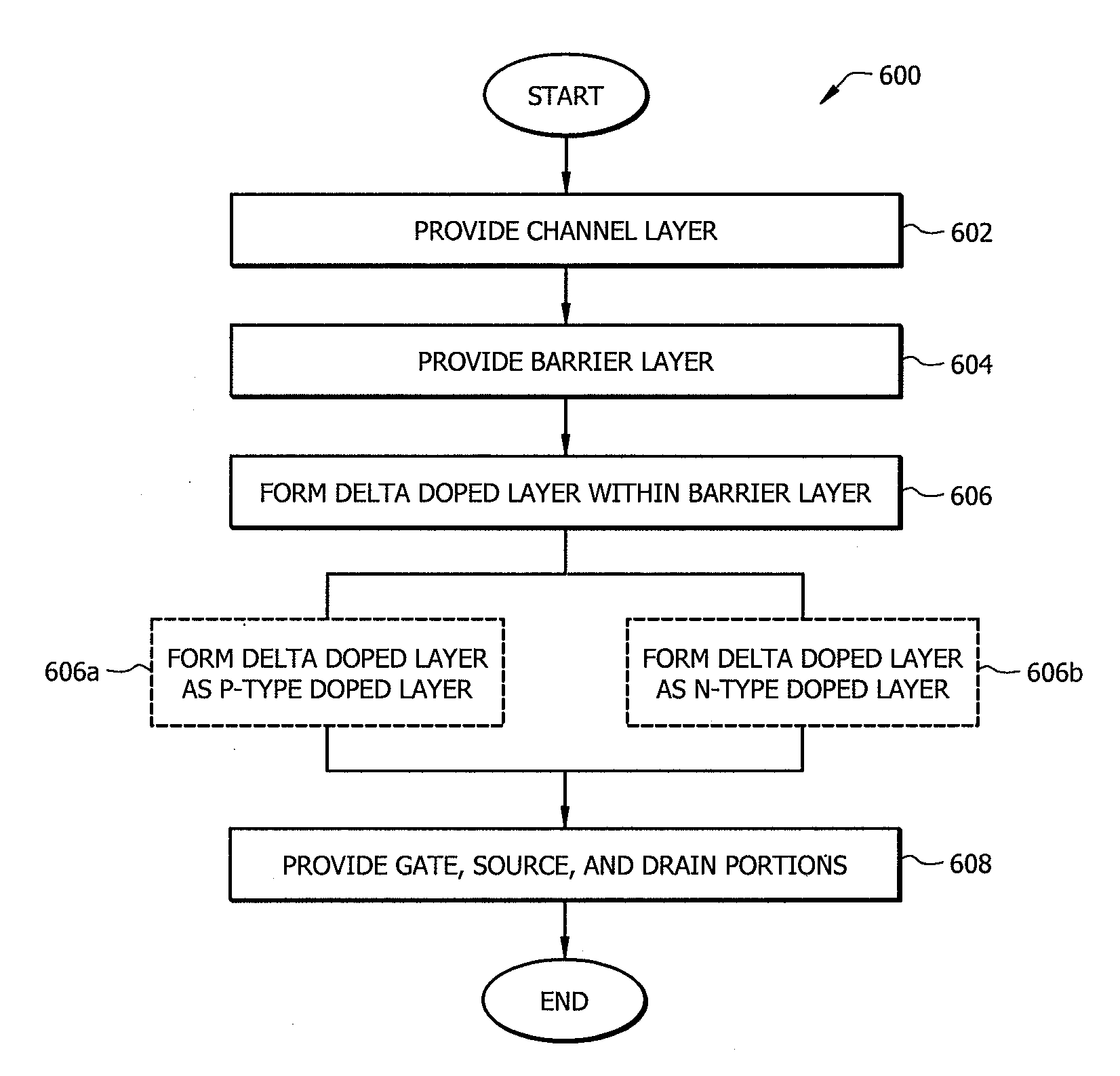
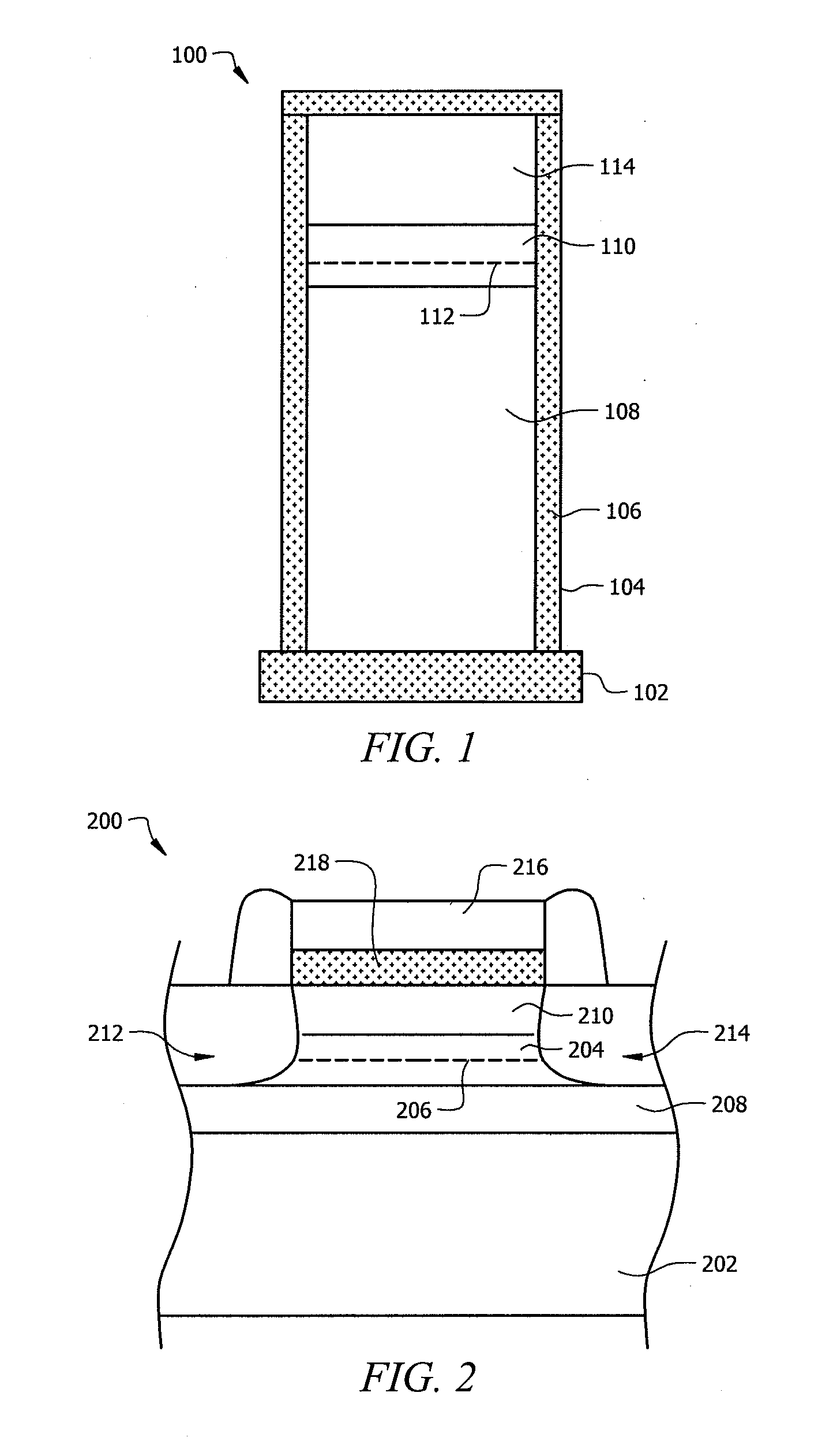
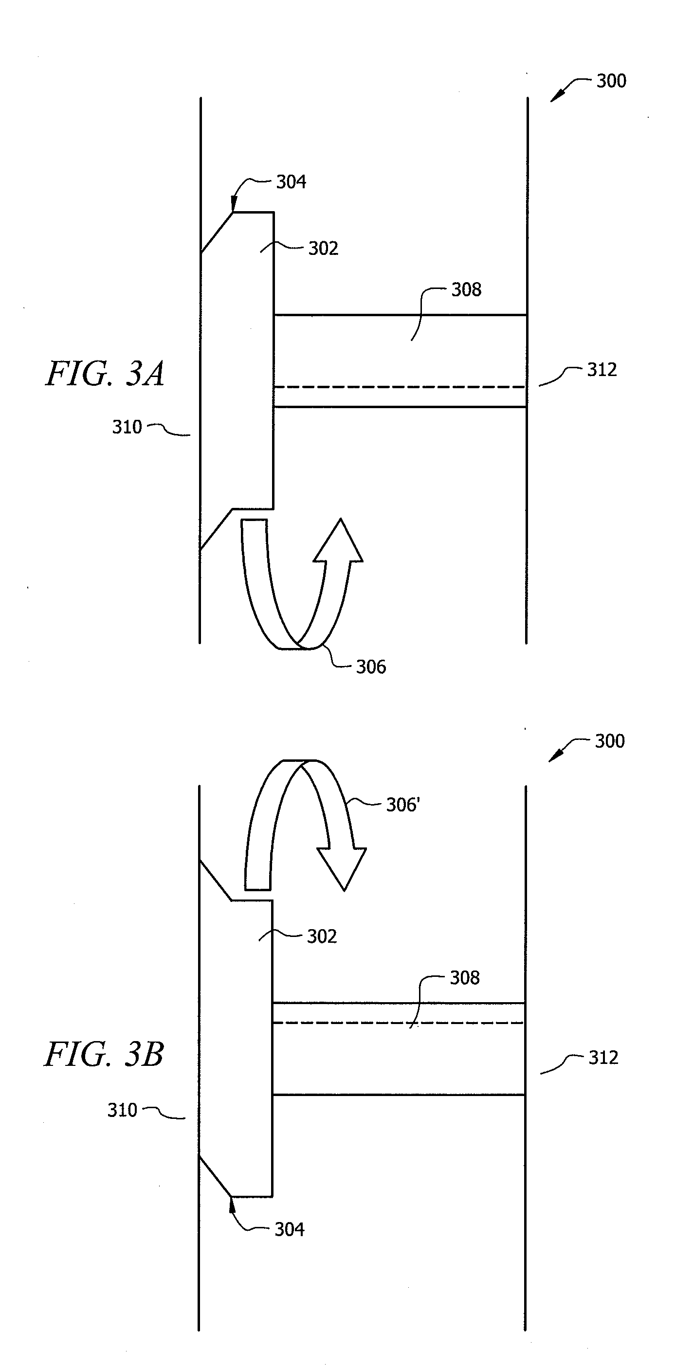
[0021]FIG. 1 illustrates one embodiment of a remote doped high performance transistor 100. Transistor 100 may include a buried oxide layer (BOX) 102, gate portion 104, and gate insulator portion 106. Ch...


PUM


Abstract

Devices comprising, and a method for fabricating, a remote doped high performance transistor having improved subthreshold characteristics are disclosed. In one embodiment a field-effect transistor includes a channel layer configured to convey between from a source portion and a drain portion of the transistor when the transistor is in an active state. Further, the field-effect transistor includes a barrier layer adjacent to the channel layer. The barrier layer comprises a delta doped layer configured to provide carriers to the channel layer of the transistor, while preferably substantially retaining dopants in said delta-doped layer.

Description

TECHNICAL FIELD[0001]This invention relates to semiconductor devices and more particularly relates to an apparatus system and method providing for a remote doped field effect transistor.BACKGROUND OF THE INVENTION[0002]In the field of semiconductor device fabrication, progress is usually gauged by a reduction in the size of semiconductor components. Unfortunately, certain semiconductor structures and materials may become unsuitable as the size decreases. More specifically in transistor design, with the reduction of channel length it is more difficult to control short channel effects. The controlling of such effects becomes even more important in high mobility channel materials due to their low band gap and poor short channel characteristics.[0003]One solution to assist in controlling short channel effects in high mobility devices is to heavily dope the channel. However, such doping eventually increases scattering, which leads to lower mobility and, thus, frustrates the main advantag...

Claims


Application Information

Patent Timeline
IPC IPC(8): H01L29/78H01L21/336H01L23/48
CPCB82Y10/00H01L21/823807H01L21/823821H01L29/205H01L29/365H01L29/775H01L2924/0002H01L29/7781H01L29/66477H01L29/7831H01L2924/00
Inventor MAJHI, PRASHANTMAJUMDAR, KAUSIK
Owner INTEL AMERICAS INC
Why Eureka
Try Eureka