Method for manufacturing semiconductor device

a semiconductor and manufacturing method technology, applied in the direction of semiconductor devices, electrical devices, transistors, etc., can solve the problem of limit on the transistor manufactured using oxide semiconductors, and achieve the effect of high field-effect mobility

Active Publication Date: 2011-06-30
SEMICON ENERGY LAB CO LTD
View PDF99 Cites 172 Cited by
  • Summary
  • Abstract
  • Description
  • Claims
  • Application Information

AI Technical Summary

Benefits of technology

[0023]A transistor having a high field-effect mobility can be manufactured and a large-sized display device, a high-performance semiconductor device, and the like are realized even when a material of a substrate serving as a base is any material such as an oxide, a nitride, or metal.

Problems solved by technology

However, there has been a limitation on the transistor manufactured using an oxide semiconductor when being used as a switching element in a driving device of a semiconductor device, for example, in a driver circuit of a large-sized display device or the like.

Method used


Image

  • Method for manufacturing semiconductor device
  • Method for manufacturing semiconductor device
  • Method for manufacturing semiconductor device

Examples


embodiment 1

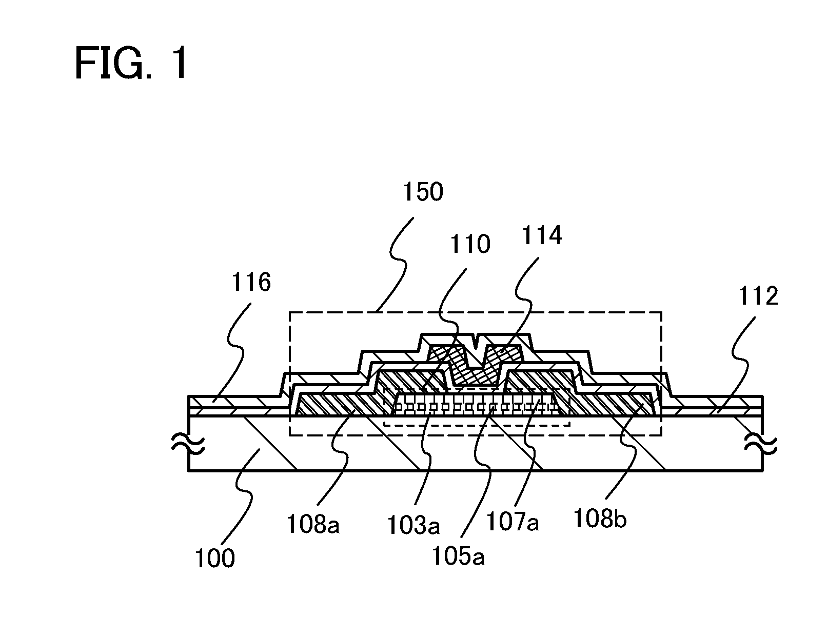
[0052]FIG. 1 is a cross-sectional view illustrating a transistor 150 which is an embodiment of a structure of a semiconductor device. Note that although the transistor 150 described here is an n-channel IGFET (insulated-gate field-effect transistor) whose carriers are electrons, the transistor 150 can be a p-channel IGFET. In this embodiment, the transistor 150 having a top gate structure will be described.

[0053]In the transistor 150 illustrated in FIG. 1, a first multi-component oxide semiconductor layer 103a including single crystal regions, a single-component oxide semiconductor layer 105a including single crystal regions, and a second multi-component oxide semiconductor layer 107a including single crystal regions are stacked over a substrate 100 (an oxide semiconductor stack), and wirings 108a and 108b functioning as a source electrode and a drain electrode are formed thereover. In addition, a gate insulating layer 112 is formed over the second multi-component oxide semiconducto...

embodiment 2

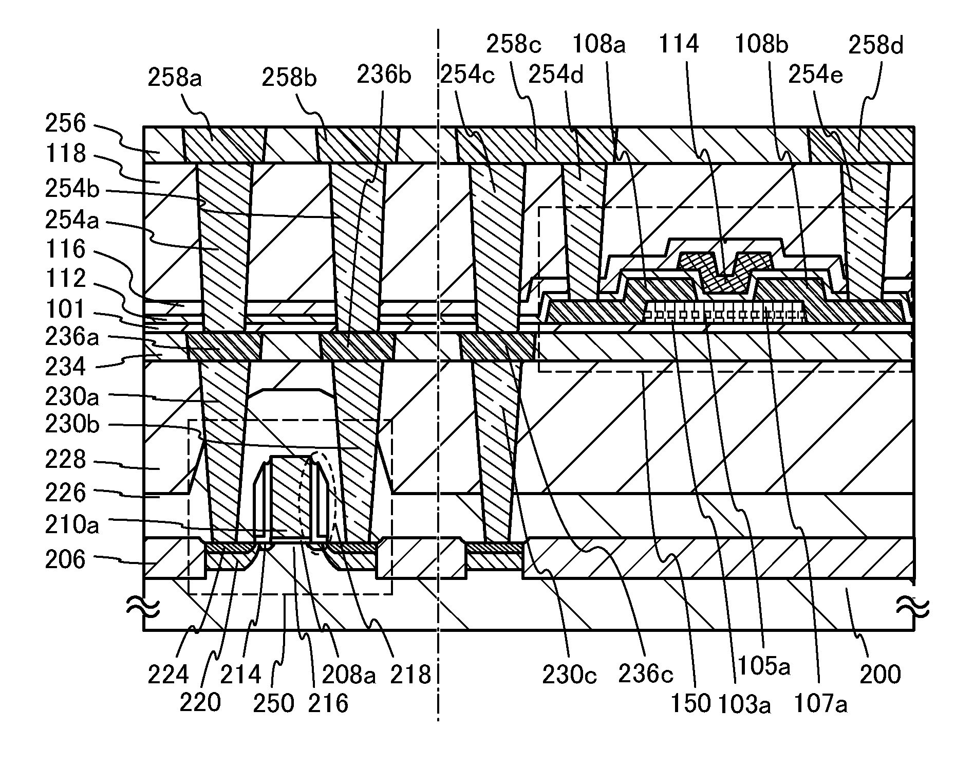
[0112]In this embodiment, a manufacturing method of a transistor including a highly purified oxide semiconductor stack will be described as a manufacturing method of a semiconductor device according to an embodiment of the invention disclosed herein with reference to FIGS. 8A to 8E, FIGS. 9A to 9D, and FIGS. 10A and 10B.

[0113]An insulating layer 101 is formed over a substrate 100. Then, in a manner similar to that in Embodiment 1, a first multi-component oxide semiconductor layer 102 is formed over the insulating layer 101, and a single-component oxide semiconductor layer 104 is formed over the first multi-component oxide semiconductor layer 102 (see FIG. 8A).

[0114]As the substrate 100, the substrate 100 described in Embodiment 1 can be used as appropriate.

[0115]The insulating layer 101 is provided so as to reduce entry of an impurity into a layer formed over the substrate 100 and to enhance adhesion to the layer formed over the substrate100. The insulating layer 101 is formed using...

embodiment 3

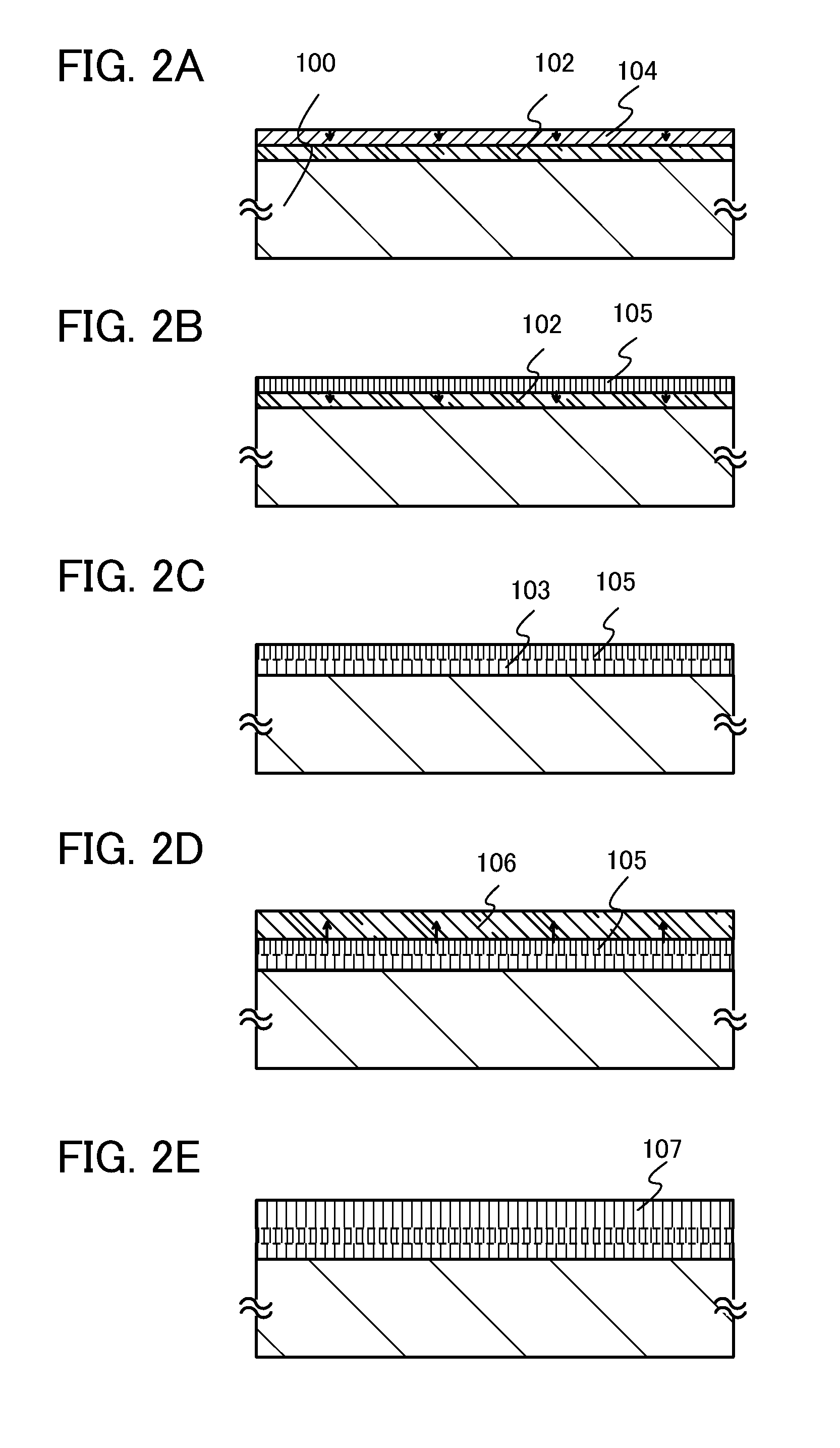
[0174]In this embodiment, a method for forming the oxide semiconductor stack 110 which is different from those in Embodiments 1 and 2 will be described with reference to FIGS. 11A to 11D.

[0175]In a manner similar to that in Embodiment 2, an insulating layer 101 is formed over a substrate 100 as illustrated in FIG. 11A. Next, a first multi-component oxide semiconductor layer 102 is formed over the insulating layer 101, and a single-component oxide semiconductor layer 104 is formed over the first multi-component oxide semiconductor layer 102.

[0176]Then, in a manner similar to that in Embodiment 1, first heat treatment is performed, so that a first multi-component oxide semiconductor layer 103 including single crystal regions and a single-component oxide semiconductor layer 105 including single crystal regions are formed as illustrated in FIG. 11B. After that, a second multi-component oxide semiconductor layer 106 is formed over the single-component oxide semiconductor layer 105 includ...


PUM


Abstract

A larger substrate can be used, and a transistor having a desirably high field-effect mobility can be manufactured through formation of an oxide semiconductor layer having a high degree of crystallinity, whereby a large-sized display device, a high-performance semiconductor device, or the like can be put into practical use. A first multi-component oxide semiconductor layer is formed over a substrate and a single-component oxide semiconductor layer is formed thereover; then, crystal growth is carried out from a surface to an inside by performing heat treatment at 500° C. to 1000° C. inclusive, preferably 550° C. to 750° C. inclusive so that a first multi-component oxide semiconductor layer including single crystal regions and a single-component oxide semiconductor layer including single crystal regions are formed; and a second multi-component oxide semiconductor layer including single crystal regions is stacked over the single-component oxide semiconductor layer including single crystal regions.

Description

TECHNICAL FIELD[0001]The present invention relates to a semiconductor device which includes a circuit including at least a semiconductor element such as a transistor as an element, and a manufacturing method thereof. For example, the present invention relates to an electronic device which includes, as a component, any of a power device mounted in a power circuit, a semiconductor integrated circuit including a memory, a thyristor, a converter, an image sensor, or the like, an electro-optical device typified by a liquid crystal display panel, and a light-emitting display device including a light-emitting element.[0002]In this specification, a semiconductor device generally means a device which can function by utilizing semiconductor characteristics, and an electro-optical device, a semiconductor circuit, and an electronic device are all semiconductor devices.BACKGROUND ART[0003]A transistor formed over a glass substrate or the like is manufactured using amorphous silicon, polycrystall...

Claims


Application Information

Patent Timeline
Patent Type & Authority Applications(United States)
IPC IPC(8): H01L29/12H01L21/20
CPCH01L21/02422H01L21/02472H01L21/02483H01L21/02502H01L29/66742H01L21/02565H01L21/02631H01L27/1225H01L29/7869H01L21/02554H01L21/84H01L27/12H01L29/04H01L29/06H01L29/66325H01L29/7393H01L21/02667H01L29/66969
Inventor YAMAZAKI, SHUNPEIHIROHASHI, TAKUYATAKAHASHI, MASAHIROSHIMAZU, TAKASHI
Owner SEMICON ENERGY LAB CO LTD
Why Eureka
Try Eureka