Parasitic Vertical PNP Bipolar Transistor in BICMOS Process

a bipolar transistor and vertical pnp technology, applied in the field of parasitic vertical pnp devices in bicmos process, can solve the problems of reduced device size, high collector resistance, and too big device size, and achieve the effect of reducing device size and parasitic resistan

Active Publication Date: 2011-06-30
SHANGHAI HUAHONG GRACE SEMICON MFG CORP
View PDF4 Cites 18 Cited by
  • Summary
  • Abstract
  • Description
  • Claims
  • Application Information

AI Technical Summary

Benefits of technology

[0005]It is therefore an objective of the present invention to offer a parasitic vertical PNP bipolar transistor with smaller device size and less conduct resistance, ready to be used for output device of BiCMOS high frequency circuit.
[0011]Present invented PNP can be used as output device of BiCMOS high frequency circuit. Deep contacts in field oxide to P type pseudo buried layer are used for collector pick-up. Compared to conventional bipolar transistors this can effectively reduce the device size. Furthermore, due to short distance of pick up to intrinsic collector, parasitic resistance is also reduced, which is very helpful for device high frequency characteristics. Other characteristics, such as current gain, will not be affected.

Problems solved by technology

The disadvantage of such structure is too big device size and high collector resistance.
STI between sinker active to intrinsic collector is necessary for such structure, which further set limit for device size reduction.

Method used


Image

  • Parasitic Vertical PNP Bipolar Transistor in BICMOS Process
  • Parasitic Vertical PNP Bipolar Transistor in BICMOS Process
  • Parasitic Vertical PNP Bipolar Transistor in BICMOS Process

Examples


Embodiment Construction

[0015]The foregoing and the object, features, and advantages of the invention will be apparent from the following detailed description of the invention, as illustrated in the accompanying drawings, in which:

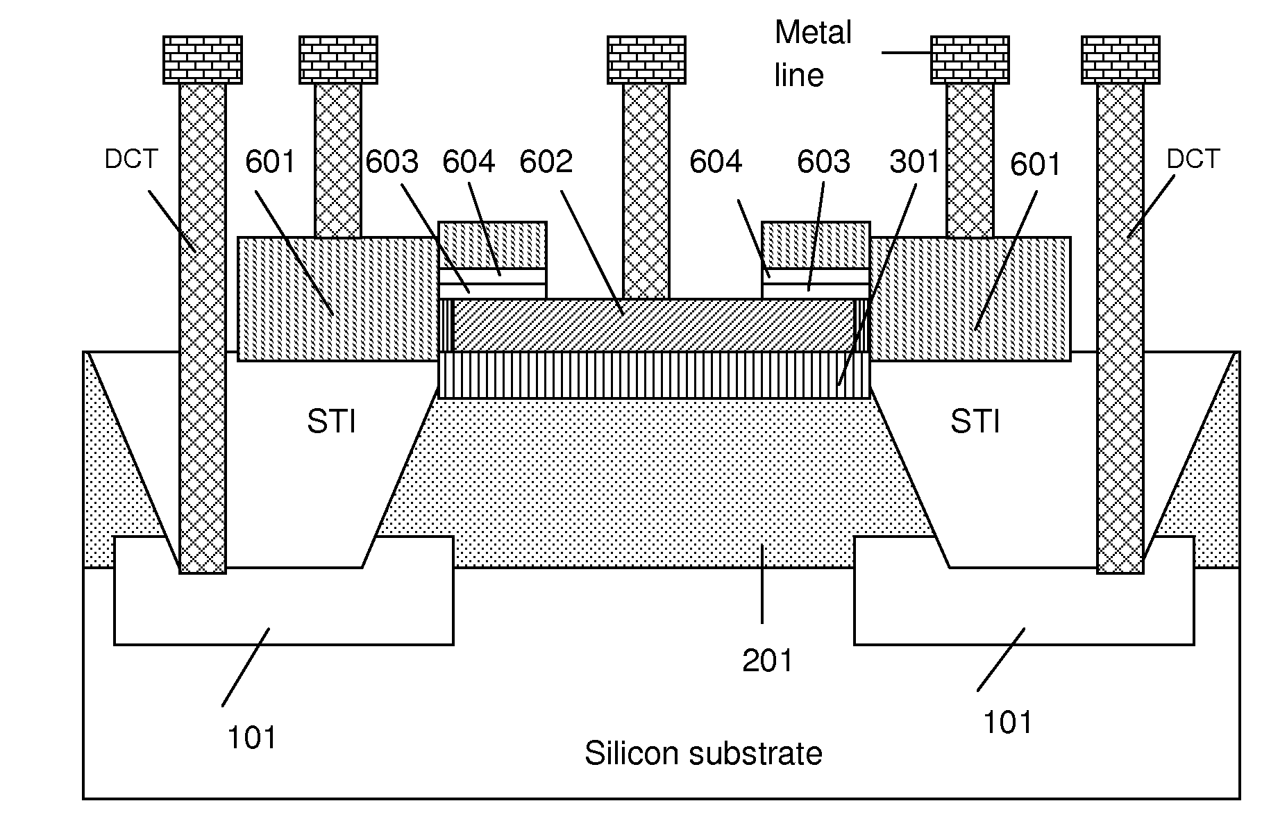
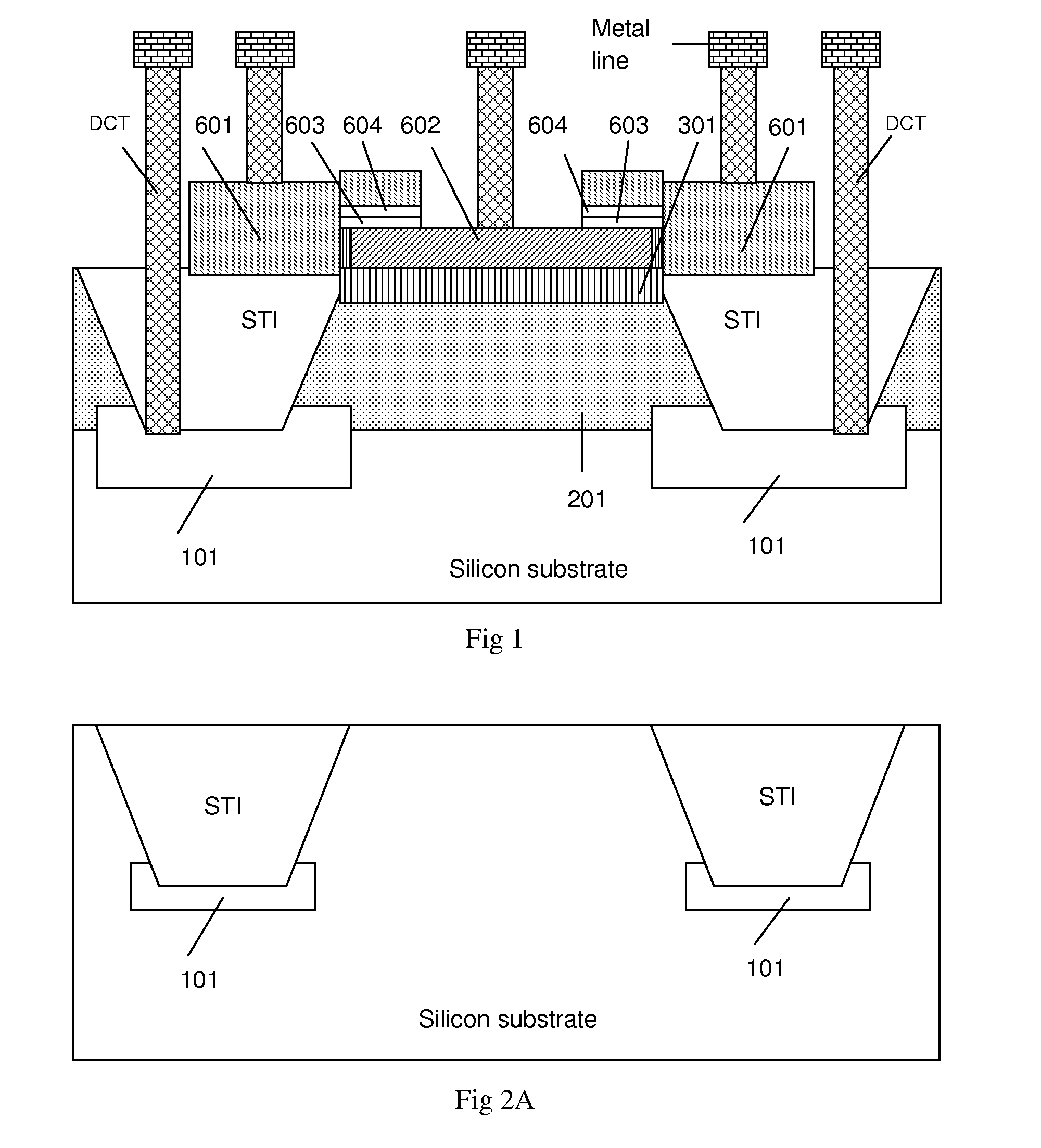
[0016]FIG. 1 is cross sectional view showing the structure of parasitic vertical bipolar transistor in BiCMOS process with shallow trench isolation. The device comprises:

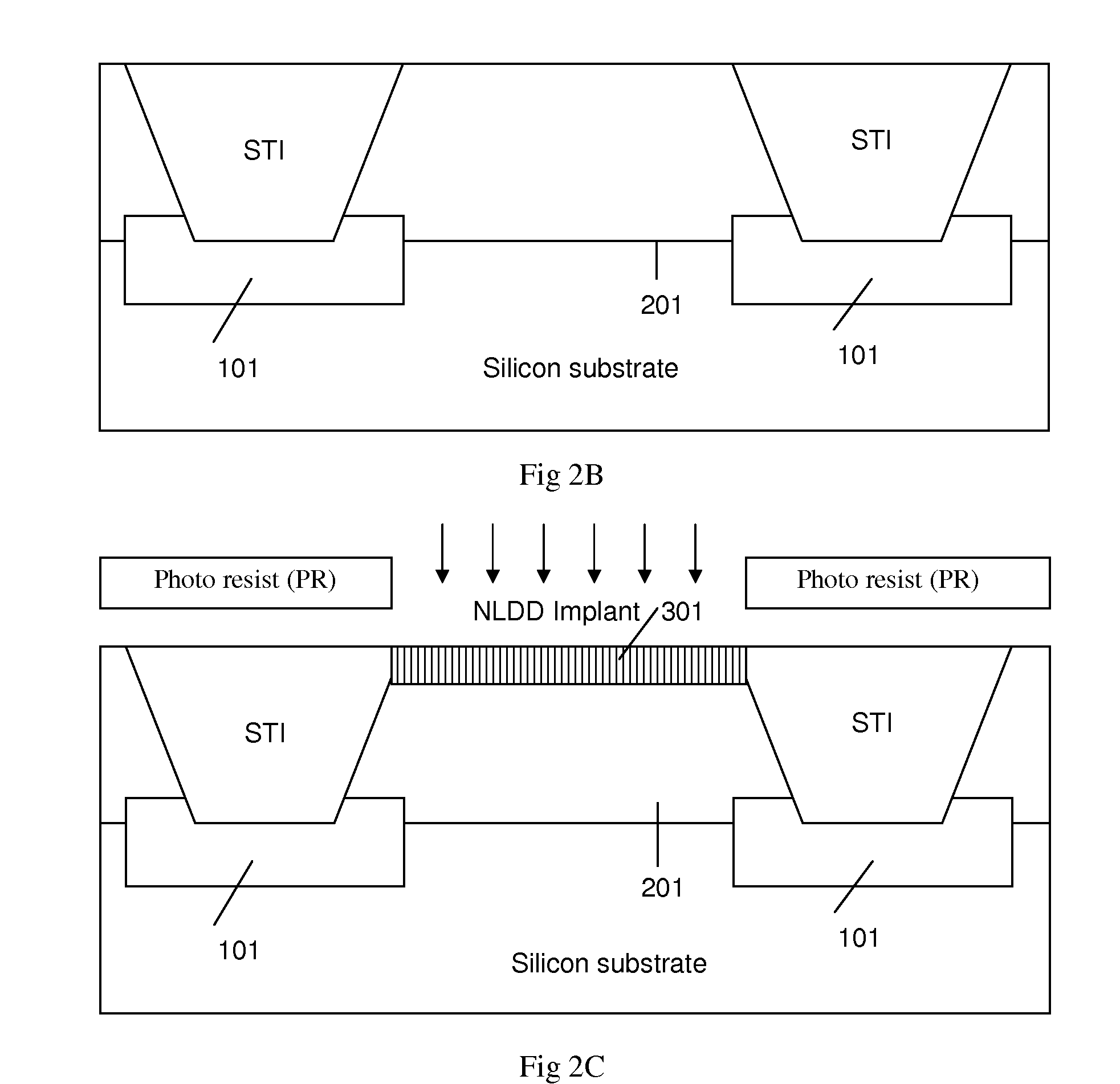
[0017]A collector 201, consist of implants of p type impurity into active area. This implanted p type impurity can adopt p well of MOSFET, or only adopt anti-punch-through and threshold implants of p well. The bottom of collector 201 connects to p type buried layer 101. P type buried layer 101 is formed at bottom of STI in both sides of collector 201 through ion implant. The ion implant dosage is range 1e14˜1e16 cm−2 and energy below 45 keV. Collector 201 is picked up by deep contacts formed by open deep contact holes through STI field oxide on top of corresponding PBL. Device collector is formed by connect a met...


PUM


Abstract

A parasitic vertical PNP device in one type of BiCMOS process with shallow trench isolation (STI) comprises a collector formed by a p type impurity ion implantation layer inside active area, the bottom of collector connects to a p type buried layer, the p type pseudo buried layer is formed in bottom of shallow trench at both sides of collector active region through ion implantation, deep contacts through field oxide to connect pseudo buried layers and to pick up the collector; a base, formed by n type impurity ion implantation layer which sits on top of above stated collector; an emitter, a p type epitaxy layer lies above base and is connected out directly by a metal contact. Part of the p type epitaxy layer is converted into n type, which serves as connection path of base. Present invented PNP can be used as output device of BiCMOS high frequency circuit. It has a small device area and conduction resistance.

Description

[0001]The current invention claims a foreign priority to the application of China 200910202067.2 filed on Dec. 31, 2009.FIELD OF THE INVENTION[0002]This invention relates generally to semiconductor devices in integrated circuits. More particularly it relates to one type of parasitic vertical PNP device in BiCMOS process.BACKGROUND OF THE INVENTION[0003]In radio frequency (RF) applications, higher and higher cut-off frequency (Ft) of RF transistor is required. Silicon bipolar junction transistor (BJT) and especially SiGeC heterojunction bipolar transistor (SiGeC HBT) are the best options of high Ft devices. As SiGe is compatible with silicon process, SiGe HBT has already become one of the mainstream ultra high frequency devices.[0004]In conventional BiCMOS process, parasitic vertical PNP bipolar transistor collector is picked up by sinker in active region to the heavily doped collector buried layer or well under STI. This approach is determined by the nature of such vertical device. ...

Claims


Application Information

Patent Timeline
Patent Type & Authority Applications(United States)
IPC IPC(8): H01L29/70
CPCH01L21/743H01L21/76224H01L21/8249H01L27/0623H01L29/0821H01L29/1004H01L29/66242H01L2924/0002H01L29/66287H01L29/732H01L29/7371H01L2924/00
Inventor CHIU, TZUYINCHU, TUNGYUANQIAN, WENSHENGFAN, YUNGCHIEHLIU, DONGHUAHU, JUN
Owner SHANGHAI HUAHONG GRACE SEMICON MFG CORP
Why Eureka
Try Eureka