Inter-phase skew detection circuit for multi-phase clock, inter-phase skew adjustment circuit, and semiconductor integrated circuit

a technology of interphase skew and detection circuit, which is applied in pulse manipulation, pulse technique, instruments, etc., can solve the problem that there is no device known for accurately implementing such reference clocks at the end of a clock distribution system

Inactive Publication Date: 2011-06-30
NEC CORP
View PDF6 Cites 43 Cited by
  • Summary
  • Abstract
  • Description
  • Claims
  • Application Information

AI Technical Summary

Benefits of technology

[0011]In light of the above circumstances, an object of the present invention is to generate reference clocks for detecting an inter-phase skew of multi-phase clocks within a semiconductor integrated circuit, so as to eliminate necessity of input of multi-phase reference clocks from an external device.
[0018]Accordingly, the reference clocks for performing the inter-phase skew detection of the multi-phase clocks can be generated within the semiconductor integrated circuit (LSI). Therefore, it is unnecessary to input reference clocks for multi-phase from an external device into an LSI, and thus it is possible to reduce skews of multi-phase clocks which function as internal clock signals, without increasing the number of external pins of the LSI.

Problems solved by technology

After the clock signals are distributed within an LSI, an offset (called “skew”) from an ideal value for the inter-phase between different phases occurs due to a difference between distributed -delays within the relevant clock tree, or a delay error caused by a dispersion between manufactured clock distribution drivers.
Therefore, a delay margin is reduced, which may cause an erroneous, operation.
However, no device for accurately implementing such reference clocks at the end of a clock distribution system is known.

Method used


Image

  • Inter-phase skew detection circuit for multi-phase clock, inter-phase skew adjustment circuit, and semiconductor integrated circuit
  • Inter-phase skew detection circuit for multi-phase clock, inter-phase skew adjustment circuit, and semiconductor integrated circuit
  • Inter-phase skew detection circuit for multi-phase clock, inter-phase skew adjustment circuit, and semiconductor integrated circuit

Examples


Embodiment Construction

[0028]Hereinafter, embodiments of the present invention will be described with reference to the appended figures.

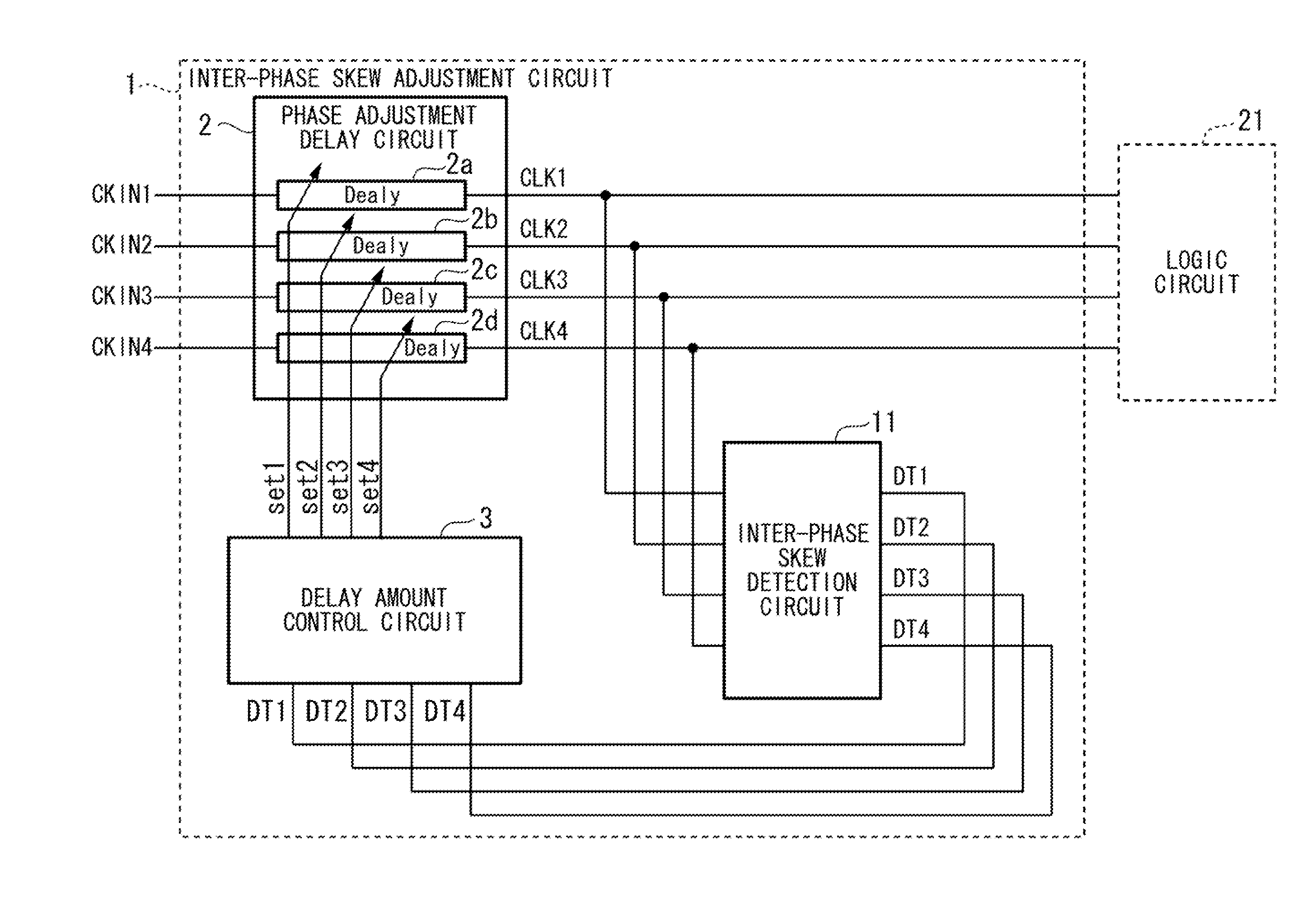
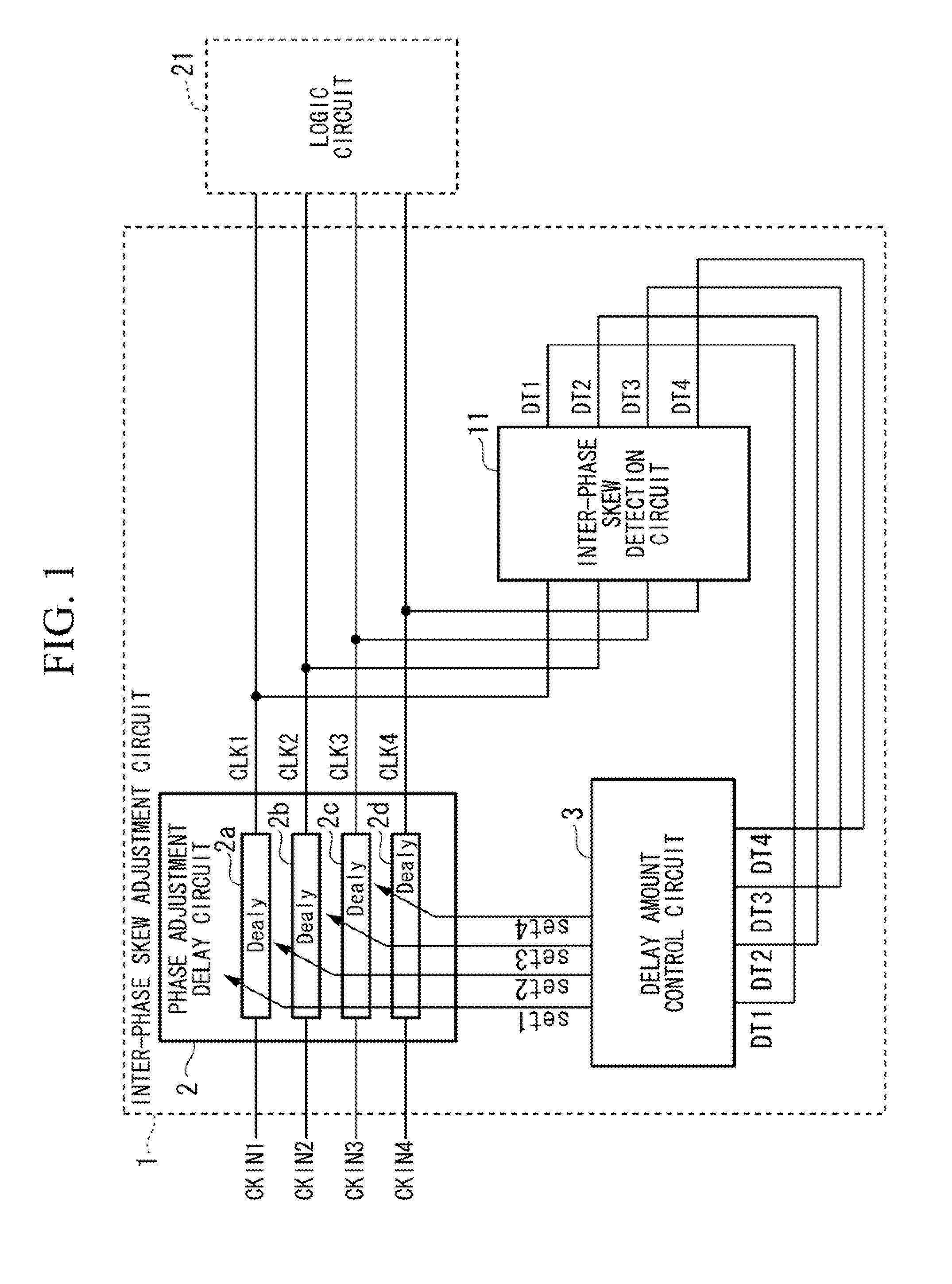
[0029]FIG. 1 is a block diagram showing the structure of an inter-phase skew adjustment circuit 1 relating to an embodiment of the present invention. The inter-phase skew adjustment circuit 1 in FIG. 1 employs 4-phase clocks (i.e., N=4 of N-phase clocks). More specifically, FIG. 1 shows a clock distribution system in a semiconductor integrated circuit, and includes a phase adjustment delay circuit 2, a delay amount control circuit 3, and an inter-phase skew detection circuit 11. In the inter-phase skew adjustment circuit 1 in FIG. 1, the phases of externally input clocks (clock signals) CKIN1, CKIN2, CKIN3, and CKIN4 of the 4-phase are each adjusted by the phase adjustment delay circuit 2, so as to generate phase-adjusted 4-phase clocks (clock signals) CLK1, CLK2, CLK3, and CLK4 (as internal clock signals), which are supplied to a logic circuit 21 in the semiconductor int...


PUM


Abstract

An inter-phase skew detection circuit includes a frequency division circuit that frequency-divides N-phase clocks to be measured at predetermined timings so as to generate N+2 frequency-divided clocks; a phase comparison target clock generation circuit that generates N phase comparison target clocks by using predetermined N frequency-divided clocks among the N+2 frequency-divided clocks; a phase comparison reference clock generation circuit that generates N reference clocks by using the N+2 frequency-divided clocks, in accordance with predetermined combinations between the N+2 frequency-divided clocks and an operation criterion; and a phase comparison circuit that detects respective phase differences between the N phase comparison target clocks and the corresponding N reference clocks.

Description

[0001]Priority is claimed on Japanese Patent Application No. 2009-298374, filed Dec. 28, 2009, the contents of which are incorporated herein by reference.BACKGROUND OF THE INVENTION[0002]1. Field of the Invention[0003]The present invention relates to an inter-phase skew detection circuit for detecting a phase offset (skew) for multi-phase clocks, an inter-phase skew adjustment circuit employing the inter-phase skew detection circuit, and a semiconductor integrated circuit (LSI) employing the inter-phase skew adjustment circuit.[0004]2. Description of the Related Art[0005]Multi-phase clocks (clock signals) such as 2-phase clocks or 4-phase clocks are used in a semiconductor integrated circuit (called an “LSI”). After the clock signals are distributed within an LSI, an offset (called “skew”) from an ideal value for the inter-phase between different phases occurs due to a difference between distributed -delays within the relevant clock tree, or a delay error caused by a dispersion betw...

Claims


Application Information

Patent Timeline
Patent Type & Authority Applications(United States)
IPC IPC(8): H03D13/00H03L7/00
CPCG01R31/31726H03L7/085H03L7/0812
Inventor HAYASHI, TOMOHIRO
Owner NEC CORP
Why Eureka
Try Eureka