Liquid crystal display device and electronic device

a display device and liquid crystal technology, applied in the field of semiconductor devices, can solve the problems of difficult to recognize display and display in the environment with strong external light, and achieve the effect of low power consumption

Active Publication Date: 2011-06-30
SEMICON ENERGY LAB CO LTD
View PDF79 Cites 64 Cited by
  • Summary
  • Abstract
  • Description
  • Claims
  • Application Information

AI Technical Summary

Benefits of technology

[0026]A liquid crystal display device in which image display can be performed in accordance with an environment of various brig

Problems solved by technology

Since the backlight is utilized in the transmissive liquid crystal display device, it is difficult to recognize display in the environment with strong external light, for example, out

Method used


Image

  • Liquid crystal display device and electronic device
  • Liquid crystal display device and electronic device
  • Liquid crystal display device and electronic device

Examples


embodiment 1

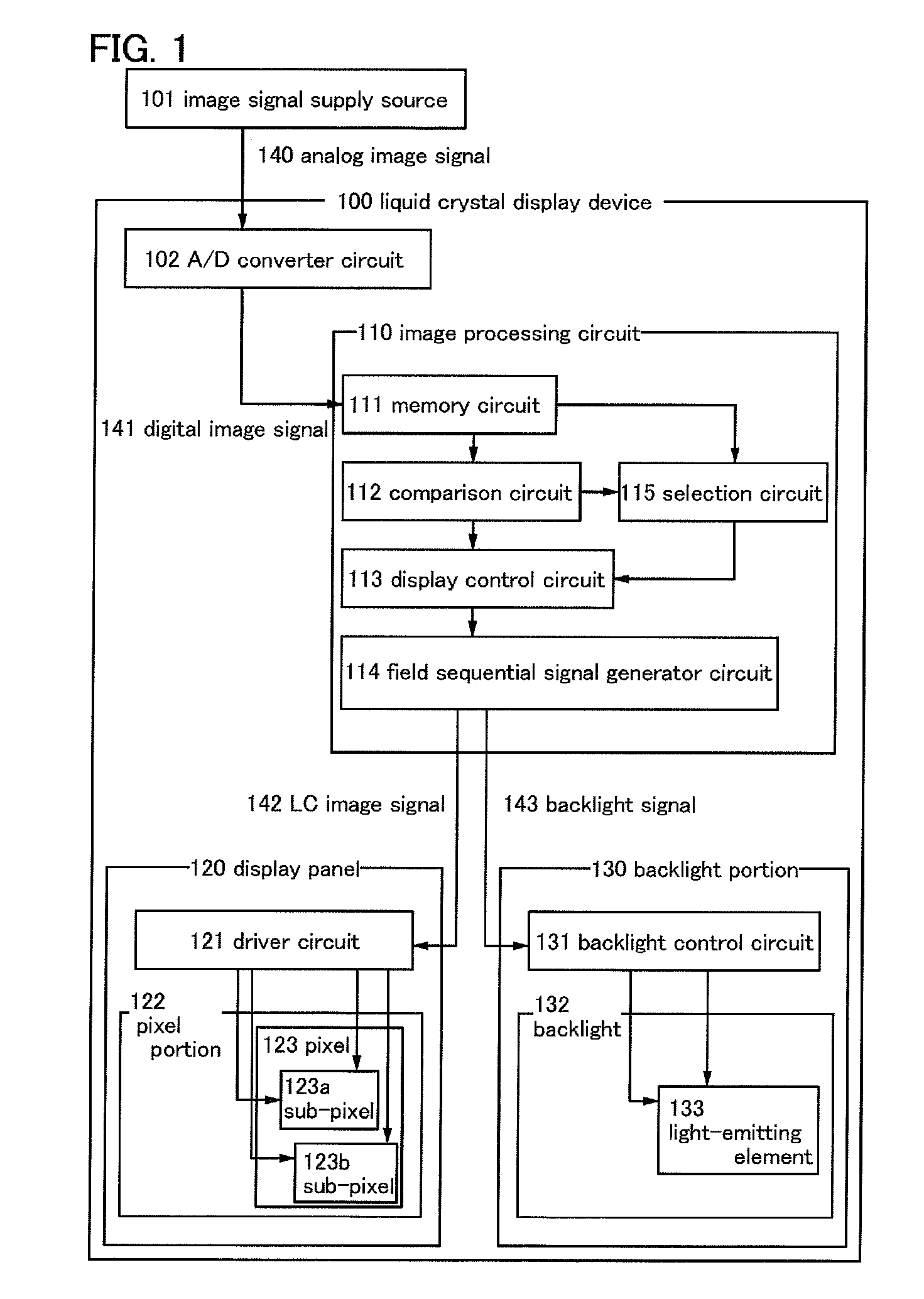
[0044]In this embodiment, a liquid crystal display device including a still-image mode and a moving-image mode will be described with reference to FIG. 1. Note that in this specification, a mode performed in such a way that a display device determines image signals input to the display device as a still image is described as a still-image mode, and a mode performed in such a way that the display device determines the image signals input to the display device as a moving image is described as a moving-image mode.

[0045]A liquid crystal display device 100 of this embodiment includes an A / D converter circuit 102, an image processing circuit 110, a display panel 120, and a backlight portion 130 (see FIG. 1).

[0046]The image processing circuit 110 includes a memory circuit 111, a comparison circuit 112, a selection circuit 115, a display control circuit 113, and a field sequential signal generator circuit 114.

[0047]The display panel 120 includes a driver circuit121 and a pixel portion 122....

embodiment 2

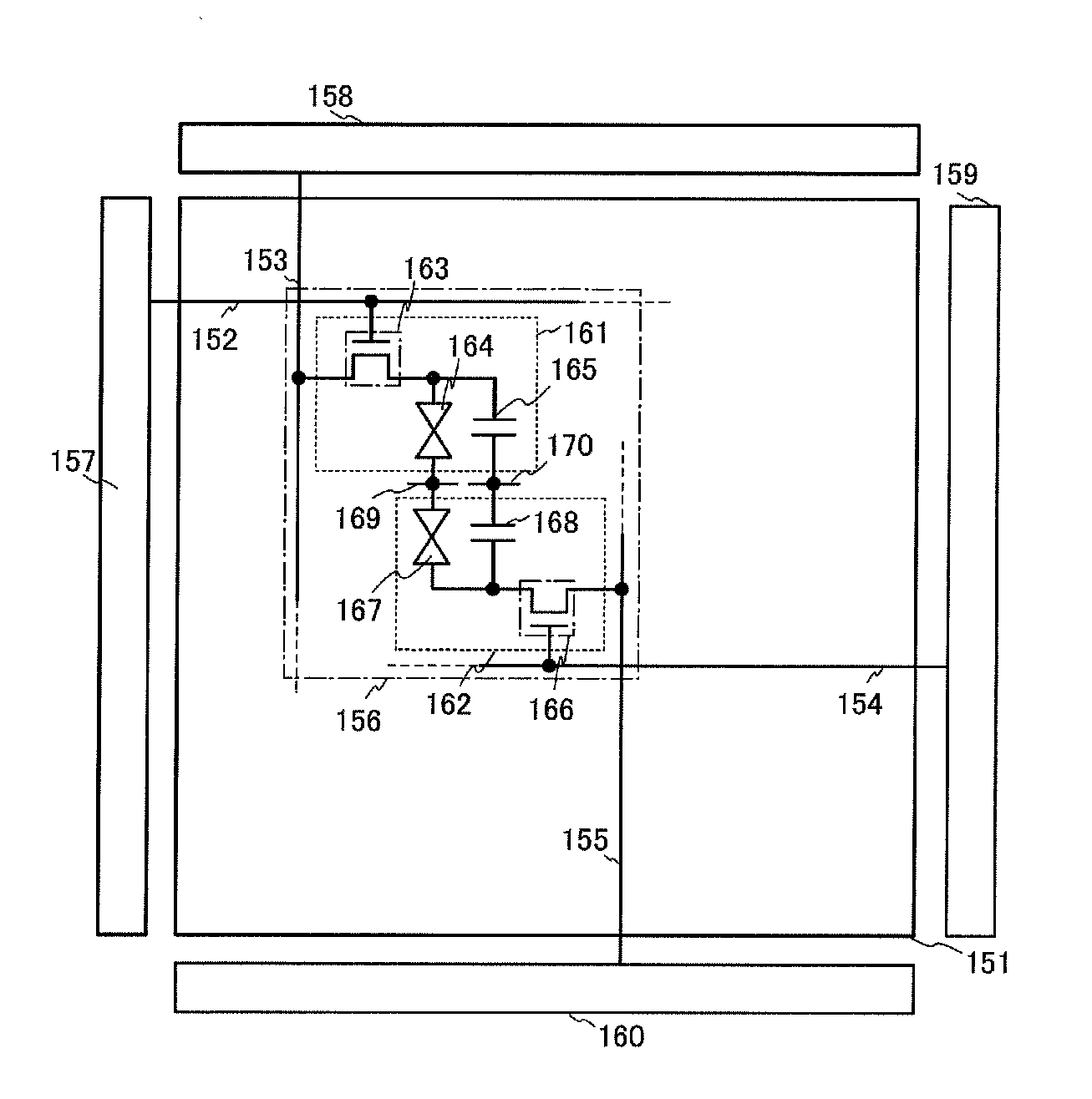
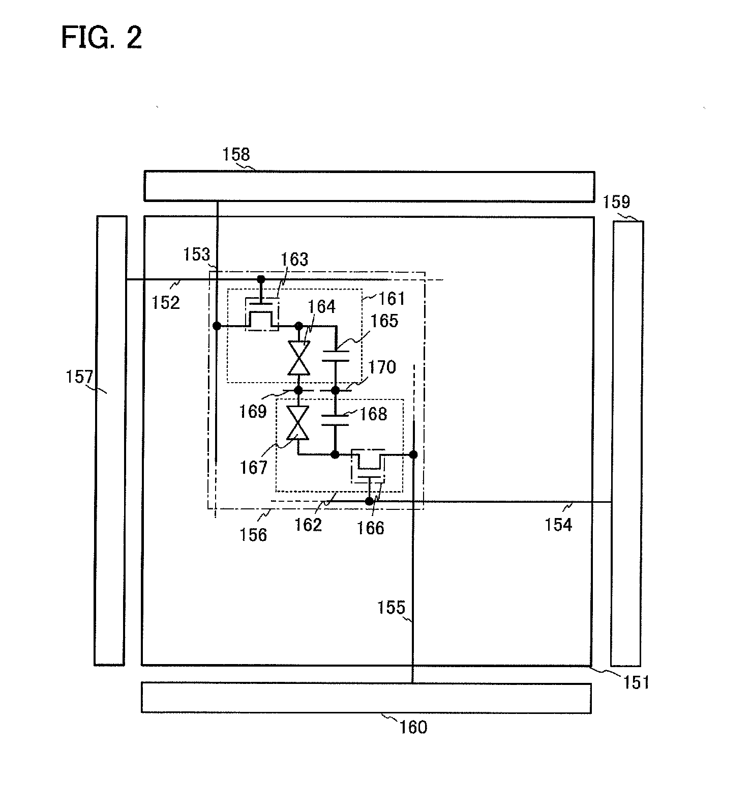
[0095]In this embodiment, a driving method of a liquid crystal display device will be described using a pixel connection diagram, a timing chart, and the like. First, FIG. 2 is a schematic view of a display panel of a liquid crystal display device. In FIG. 2, the display panel includes a pixel portion 151, a first scan line 152 (also referred to as a gate line), a first signal line 153 (also referred to as a data line), a second scan line 154, a second signal line 155, a pixel 156, a common electrode 169, a capacitor line 170, a first scan line driver circuit 157, a first signal line driver circuit 158, a second scan line driver circuit 159, and a second signal line driver circuit 160.

[0096]The pixel 156 is roughly divided into a light-transmitting electrode portion 161 and a reflective electrode portion 162. The light-transmitting electrode portion 161 includes a pixel transistor 163, a liquid crystal element 164, and a capacitor 165. A gate of the pixel transistor 163 is connected...

embodiment 3

[0117]In this embodiment, a driving method which is different from the driving method of the liquid crystal display device described in Embodiment 2 will be described with reference to a timing chart and the like. First, a driving method of the backlight in the moving-image display period 301 described in Embodiment 2 will be described using a timing chart in FIG. 4A.

[0118]The timing chart in FIG. 4A is different from that of FIG. 3B in that a non-lighting period (BL of FIG. 4A) of the backlight is provided after the backlight is turned on, following the writing of the image signal. The non-lighting period of the backlight is provided before writing of the next image signal, so that a flicker of color or the like can be reduced and visibility can be improved.

[0119]FIG. 4B illustrates a structure different from that in FIG. 4A. The timing chart in FIG. 4B is different from that of FIG. 4A in that a B (blue) light-emitting period is provided instead of the non-lighting period BL of th...


PUM


Abstract

To provide a liquid crystal display device which can perform image display in both modes: a reflective mode where external light is used as an illumination light source; and a transmissive mode where a backlight is used. In one pixel, a region where incident light through a liquid crystal layer is reflected to perform display (reflective region) and a region through which light from the backlight passes to perform display (transmissive region) are provided, and image display can be performed in both modes: the reflective mode where external light is used as an illumination light source; and the transmissive mode where the backlight is used as an illumination light source. In addition, two transistors connected to respective pixel electrode layers are provided in one pixel, and the two transistors are separately operated, whereby display of the reflective region and display of the transmissive region can be controlled independently.

Description

TECHNICAL FIELD[0001]The present invention relates to a semiconductor device having a circuit formed using a transistor and a manufacturing method thereof. The present invention relates to, for example, an electronic device on which an electro-optical device typified by a liquid crystal display panel is mounted as a component.BACKGROUND ART[0002]In a liquid crystal display device, an active matrix liquid crystal display device, in which pixel electrodes are provided in matrix and transistors are used as switching elements connected to respective pixel electrodes in order to obtain an image with high quality, has attracted attention.[0003]An active matrix liquid crystal display device, in which transistors formed using a metal oxide for a channel formation region are used as switching elements connected to respective pixel electrode, has already been known (see Patent Document 1 and Patent Document 2).[0004]It is known that an active matrix liquid crystal display device is classified...

Claims


Application Information

Patent Timeline
IPC IPC(8): G09G3/36G09G5/02
CPCG02F1/133553G09G3/3648G09G2320/10G09G2310/063G09G2300/0456G02F1/133621G09G2310/0235G02F1/1368G09G3/36
Inventor YAMAZAKI, SHUNPEIKOYAMA, JUNHIRAKATA, YOSHIHARU
Owner SEMICON ENERGY LAB CO LTD
Why Eureka
Try Eureka