Hybrid silicon vertical cavity laser with in-plane coupling

a laser structure and vertical cavity technology, applied in semiconductor lasers, instruments, optical elements, etc., can solve the problems of inefficient light emission of silicon, inability to efficiently generate large amounts of light, and heat generation of silicon

Inactive Publication Date: 2011-06-30
INTEL CORP
View PDF4 Cites 50 Cited by
  • Summary
  • Abstract
  • Description
  • Claims
  • Application Information

AI Technical Summary

Problems solved by technology

Although silicon is an excellent material for guiding light and can detect and modulate light at high data rates, it has not yet been capable of efficiently generating large amounts of light.
Silicon may be an inefficient light emitter because of a fundamental limitation called an indirect bandgap.
Instead, silicon tends to emit heat.
However, there are some inherent di

Method used


Image

  • Hybrid silicon vertical cavity laser with in-plane coupling
  • Hybrid silicon vertical cavity laser with in-plane coupling
  • Hybrid silicon vertical cavity laser with in-plane coupling

Examples


Embodiment Construction

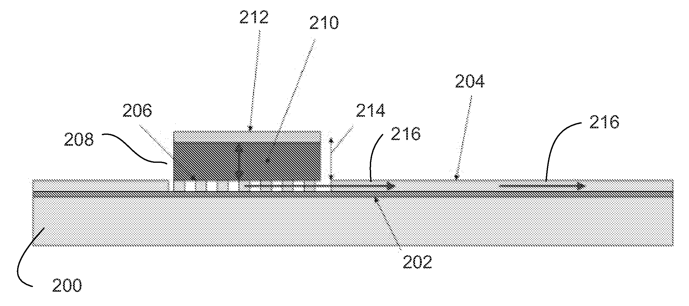
[0012]Described is a VCSEL-like laser on silicon. By combining the high efficiency and modulation bandwidth of vertical cavity lasers with the light guiding, multiplexing, detecting, and modulating capabilities of in-plane silicon photonics advantages may be obtained.

[0013]Reference throughout this specification to “one embodiment” or “an embodiment” means that a particular feature, structure, or characteristic described in connection with the embodiment is included in at least one embodiment of the present invention. Thus, the appearances of the phrases “in one embodiment” or “in an embodiment” in various places throughout this specification are not necessarily all referring to the same embodiment. Furthermore, the particular features, structures, or characteristics may be combined in any suitable manner in one or more embodiments.

[0014]Referring now to FIG. 2, embodiments of the invention involve wafer bonding an active III-V semiconductor material above a grating coupler made on ...


PUM


Abstract

A silicon vertical cavity laser with in-plane coupling comprises wafer bonding an active III-V semiconductor material above a grating coupler made on a silicon-on-insulator (SOI) wafer. This bonding does not require any alignment, since all silicon processing can be done before bonding, and all III-V processing can be done after bonding. The grating coupler acts to couple the vertically emitted light from the hybrid vertical cavity into a silicon waveguide formed on an SOI wafer.

Description

FIELD OF THE INVENTION[0001]Embodiments of the present invention are directed to vertical cavity lasers and, more particularly, to hybrid silicon / III-V vertical cavity laser structures for use in in-plane, waveguide based photonic integrated circuits.BACKGROUND INFORMATION[0002]Although silicon is an excellent material for guiding light and can detect and modulate light at high data rates, it has not yet been capable of efficiently generating large amounts of light. Silicon may be an inefficient light emitter because of a fundamental limitation called an indirect bandgap. An indirect bandgap prevents the atoms in silicon from emitting photons in large numbers when an electrical charge is applied. Instead, silicon tends to emit heat.[0003]One approach to generate light on a silicon material is the so-called hybrid silicon evanescent platform. Indium Phosphide is one of a few special materials, including Gallium Arsenide, which emits energy as a photon of light when voltage is applied...

Claims


Application Information

Patent Timeline
IPC IPC(8): H01S5/026H01L21/28H01L31/0304
CPCG02B6/124G02B6/4204H01S5/0215H01S5/02248H01S5/1838H01S5/0268H01S5/026H01S5/105H01S5/1032H01S5/183H01S5/02325H01S5/11
Inventor KOCH, BRIAN R.
Owner INTEL CORP
Why Eureka
Try Eureka