SELF-ALIGNED COMPOSITE M-MOx/DIELECTRIC CAP FOR Cu INTERCONNECT STRUCTURES

a dielectric cap and self-aligning technology, which is applied in the direction of resistive material coating, printed circuit non-printed electric components association, plasma technique, etc., can solve the problems of affecting the electromigration of the cu-containing interconnect structure, the thickness of the co-containing alloy is difficult to reduce to a sub-5 nm range by conventional wet plating process, and the effect of reducing the thickness of the metal cap

Active Publication Date: 2011-07-07
AURIGA INNOVATIONS INC
View PDF5 Cites 20 Cited by
  • Summary
  • Abstract
  • Description
  • Claims
  • Application Information

AI Technical Summary

Benefits of technology

[0010]In one embodiment of the invention, a self-aligned composite metal (M)-metal oxide (MOx) cap is employed within a Cu-containing interconnect structure. The presence of the self-aligned composite M-MOx cap improves the electromigration of a Cu-containing interconnect structure while reducing the metal cap thickness to a sub-5 nm range to minimize the resistance increase to the Cu-containing interconnect structure. In addition, the metal film that is deposited on the Cu surface will react with any oxygen residue present within the Cu feature to form a stable MOx region at the Cu interface that will remain in the structure even after a thermal or low rf power reducing plasma cleaning process. A dielectric cap is subsequently formed to protect the surface of the M region of the M-MOx cap from oxidizing in air and to provide an etch / CMP stop surface during subsequent processes.

Problems solved by technology

The EM initial voids first nucleate at the metal / dielectric cap interface and then grow in the direction to the bottom of the interconnect, which eventually results in a circuit dead opening.
Although metal caps can improve the electromigration resistance of the interconnect structure, prior art metal cap plating processes have some drawbacks associated therewith.
For example, it is difficult to reduce the thickness of a Co-containing alloy to a sub-5 nm range by conventional wet plating processes.
Moreover, conventional wet plating processes that are typically used in forming Co-containing alloy caps may have a detrimental impact by absorption to high porosity (greater than 25% porosity) ultra low k porous SiCOH dielectric films that are being presently implemented in sub-32 nm interconnect structures.
Furthermore, the selective plating of Co-containing alloy caps is not perfectly selective and some of the cap material may extend onto the dielectric surface creating shorts in the interconnect structure.
It is also worth mentioning that during a clean in dilute hydrofluoric acid, which is generally used to clean the surface of the interconnect dielectric material, corrosion of metal caps may occur.
Moreover, the current high rf power reducing plasmas that are also used to clean the Cu surface prior to dielectric deposition or Co-containing alloy plating will cause substantial damage to the underlying low k dielectric material surface and degrade both the electrical and mechanical properties.

Method used


Image

  • SELF-ALIGNED COMPOSITE M-MOx/DIELECTRIC CAP FOR Cu INTERCONNECT STRUCTURES
  • SELF-ALIGNED COMPOSITE M-MOx/DIELECTRIC CAP FOR Cu INTERCONNECT STRUCTURES
  • SELF-ALIGNED COMPOSITE M-MOx/DIELECTRIC CAP FOR Cu INTERCONNECT STRUCTURES

Examples


Embodiment Construction

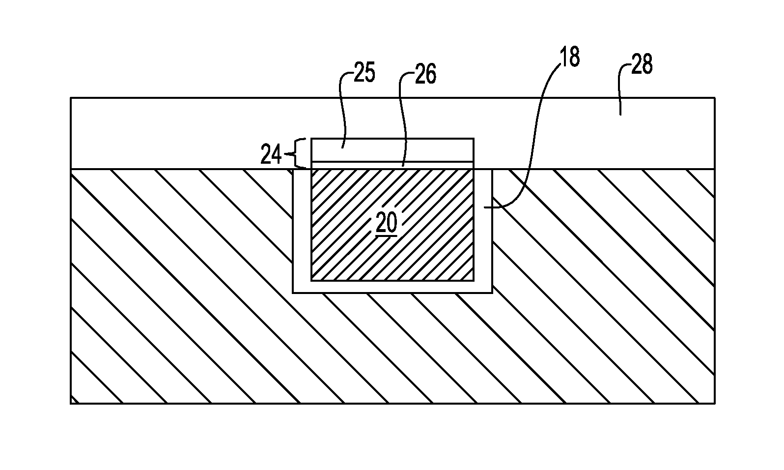
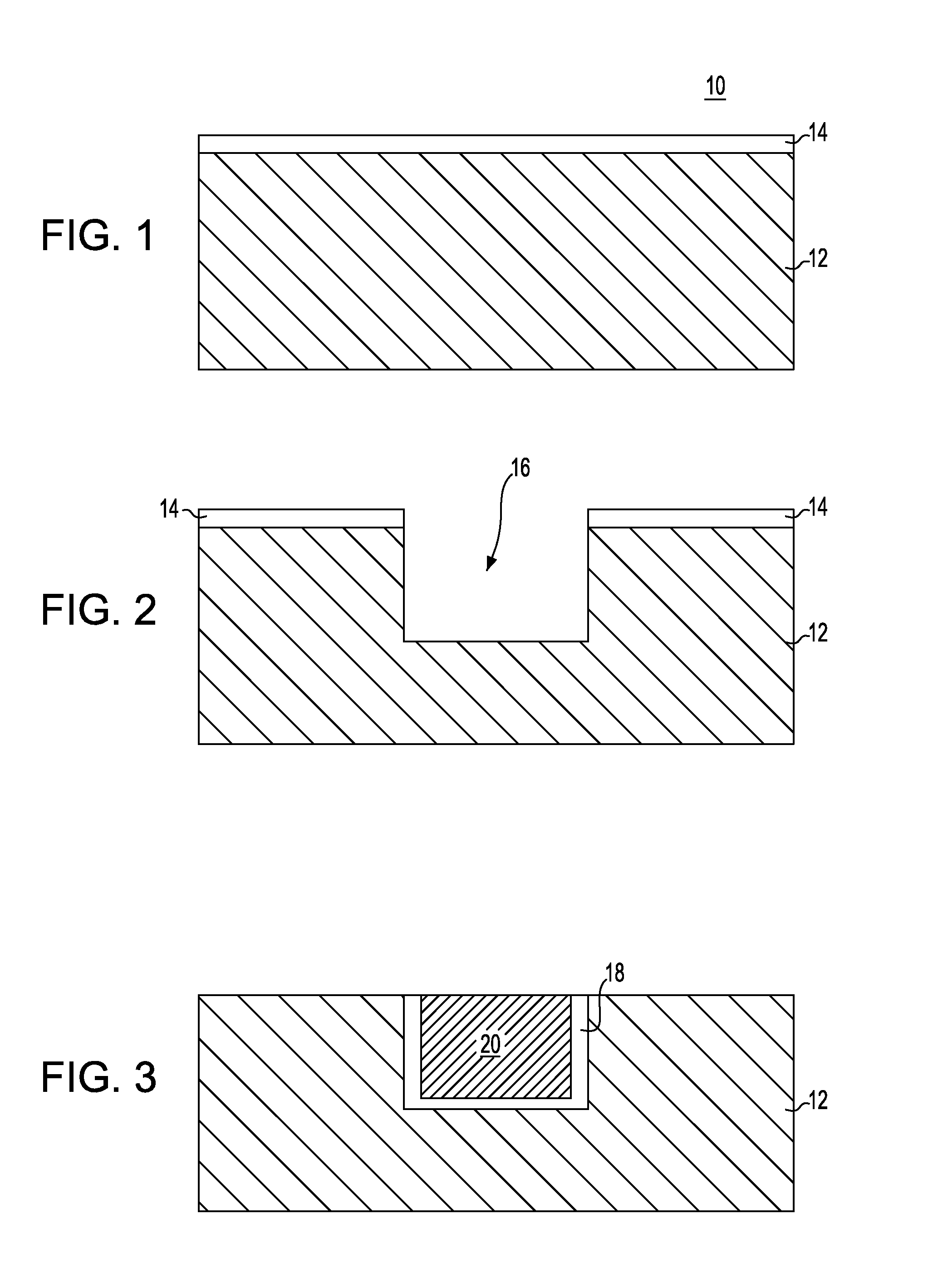
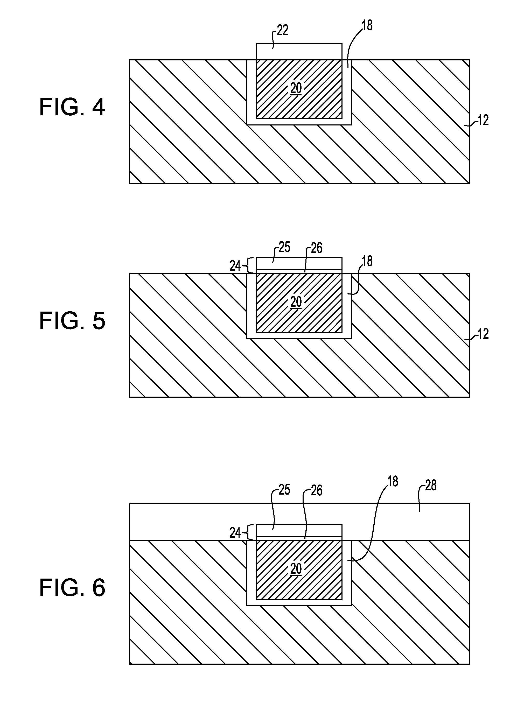
[0022]The present invention, which provides an interconnect structure having enhanced electromigration (EM) reliability and methods of forming the same, will now be described in greater detail by referring to the following discussion and drawings that accompany the present application. It is noted that the drawings of the present application are provided for illustrative purposes only and, as such, the drawings are not drawn to scale.

[0023]In the following description, numerous specific details are set forth, such as particular structures, components, materials, dimensions, processing steps and techniques, in order to provide a thorough understanding of the present invention. However, it will be appreciated by one of ordinary skill in the art that the invention may be practiced without these specific details. In other instances, well-known structures or processing steps have not been described in detail in order to avoid obscuring the invention.

[0024]It will be understood that when ...


PUM

PropertyMeasurementUnit
dielectric constantaaaaaaaaaa
porosityaaaaaaaaaa
dielectric constantaaaaaaaaaa

Abstract

An interconnect structure is provided that has improved electromigration resistance as well as methods of forming such an interconnect structure. The interconnect structure includes an interconnect dielectric material having a dielectric constant of about 4.0 or less. The interconnect dielectric material has at least one opening therein that is filled with a Cu-containing material. The Cu-containing material within the at least one opening has an exposed upper surface that is co-planar with an upper surface of the interconnect dielectric material. The interconnect structure further includes a composite M-MOx cap located at least on the upper surface of the Cu-containing material within the at least one opening. The composite M-MOx cap includes an upper region that is composed of the metal having a higher affinity for oxygen than copper and copper oxide and a lower region that is composed of a non-stoichiometric oxide of said metal. The interconnect structure further includes a dielectric cap located on at least an upper surface of the composite M-MOx cap.

Description

BACKGROUND[0001]The present invention relates to an interconnect structure and methods of fabricating the same. More particularly, the present invention relates to an interconnect structure having enhanced electromigration reliability in which a composite metal (M)-metal oxide (MOx) / dielectric cap is employed.[0002]Generally, semiconductor devices include a plurality of circuits that form an integrated circuit (IC) fabricated on a semiconductor substrate. A complex network of signal paths will normally be routed to connect the circuit elements distributed on the surface of the substrate. Efficient routing of these signals across the device requires formation of multilevel or multilayered schemes, such as, for example, single or dual damascene wiring structures. The wiring structure typically includes copper, Cu, since Cu based interconnects provide higher speed signal transmission between large numbers of transistors on a complex semiconductor chip as compared with aluminum, Al, bas...

Claims


Application Information

Patent Timeline
Patent Type & Authority Applications(United States)
IPC IPC(8): H05K1/09B05D5/12B05D3/06B05D3/04
CPCH01L21/76846H01L21/76867H01L21/76864H01L21/76849
Inventor NGUYEN, SON VANGRILL, ALFREDHAIGH, JR., THOMAS J.SHOBHA, HOSADURGAVO, TUAN A.
Owner AURIGA INNOVATIONS INC
Why Eureka
Try Eureka