Method for Fabricating Optical Semiconductor Tubes and Devices Thereof

a technology of optical semiconductor tubes and manufacturing methods, applied in the direction of nanotechnology, electrical equipment, lasers, etc., can solve the problems of difficult low-pass threshold operation, high efficiency, and difficult to achieve high-efficiency, and achieve high-pass threshold operation, etc., to achieve the effect of direct growth of optical semiconductor tubes or inability to achieve direct growth

Active Publication Date: 2011-07-07
MCGILL UNIV
View PDF3 Cites 32 Cited by
  • Summary
  • Abstract
  • Description
  • Claims
  • Application Information

AI Technical Summary

Problems solved by technology

However, their practical applications have been limited, to a large extent, by the generation and propagation of dislocations, due to the large lattice and thermal mismatches between III-V materials and Si.
The realization of such devices, however, generally involves the use of fairly complicated top-down fabrication processes and to date has been limited to devices that operate at low temperatures and / or pulsed modes.
Although electrically injected microdisk, microcylinder, and photonic crystal based devices have been extensively investigated, the achievement of high efficiency, highly reliable, and low threshold operation has remained challenging.
It would also be evident that in many applications direct growth of the optical semiconductor tubes would either not be feasible through processing incompatibilities, performance requirements, etc or that the substrate area required for their fabrication that is then not exploited in the final device.
In spite of the significant progress made in dry printing, wafer bonding, solution casting, and more recently substrate-on-substrate (SOS) transfer processes, the reliable transfer of a high-quality optical microcavity on a foreign substrate has hitherto not been achieved.
These techniques have been limited, to a large extent, by the unique properties of these optical micro- and nanocavities, which generally rely on the use of free-standing nanomembranes.
Consequently, the commonly used dry printing and / or stamping techniques may significantly alter the structural and optical properties of the devices.
The presence of a large surface tension for conventional photonic crystal, microdisk, and micropillar devices also makes it extremely difficult to detach the cavities from the handling substrate.
However, a controlled transfer and exact positioning of single micro- and nanotube devices has not been possible with these techniques.

Method used


Image

  • Method for Fabricating Optical Semiconductor Tubes and Devices Thereof
  • Method for Fabricating Optical Semiconductor Tubes and Devices Thereof
  • Method for Fabricating Optical Semiconductor Tubes and Devices Thereof

Examples


Embodiment Construction

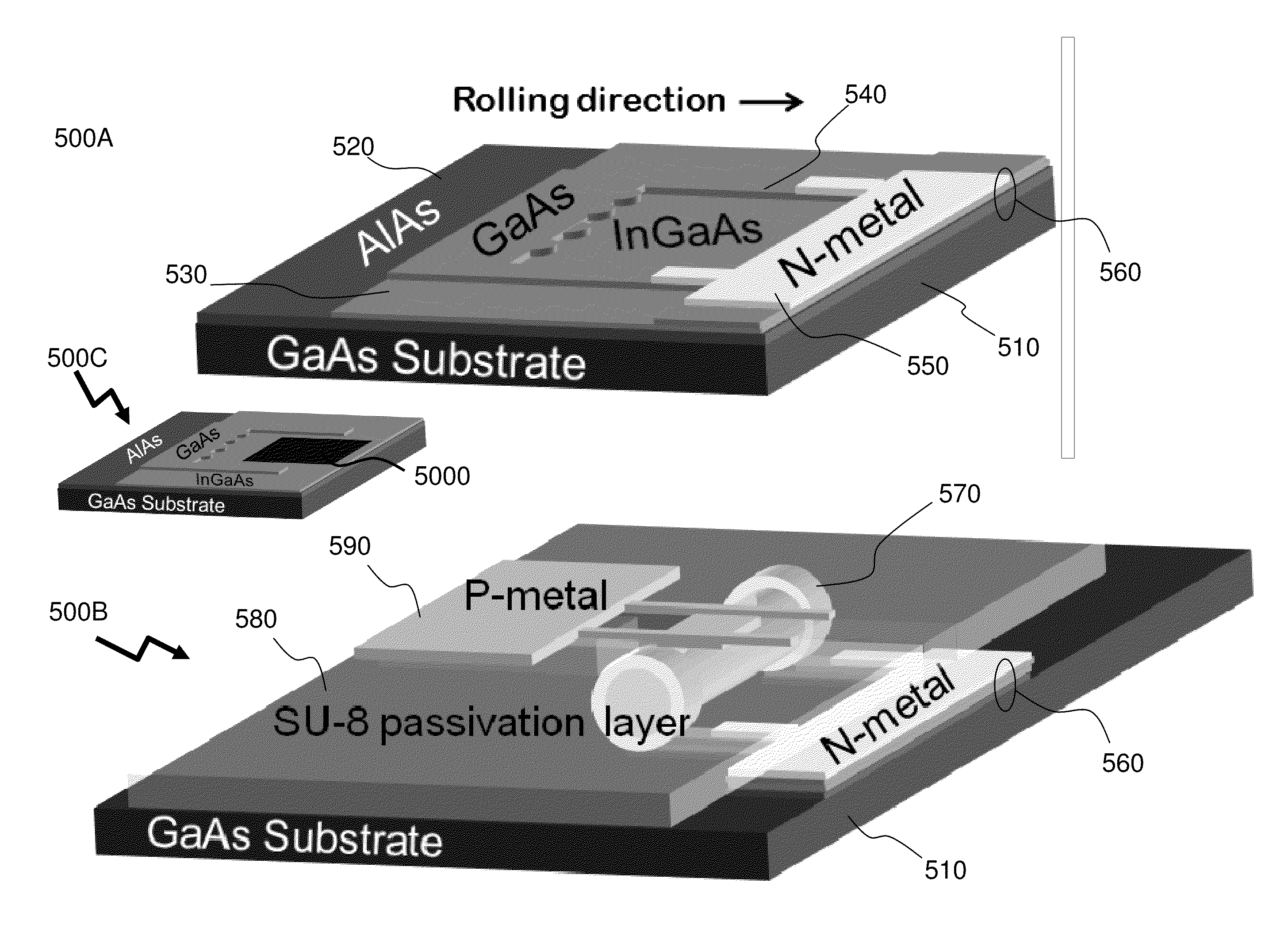
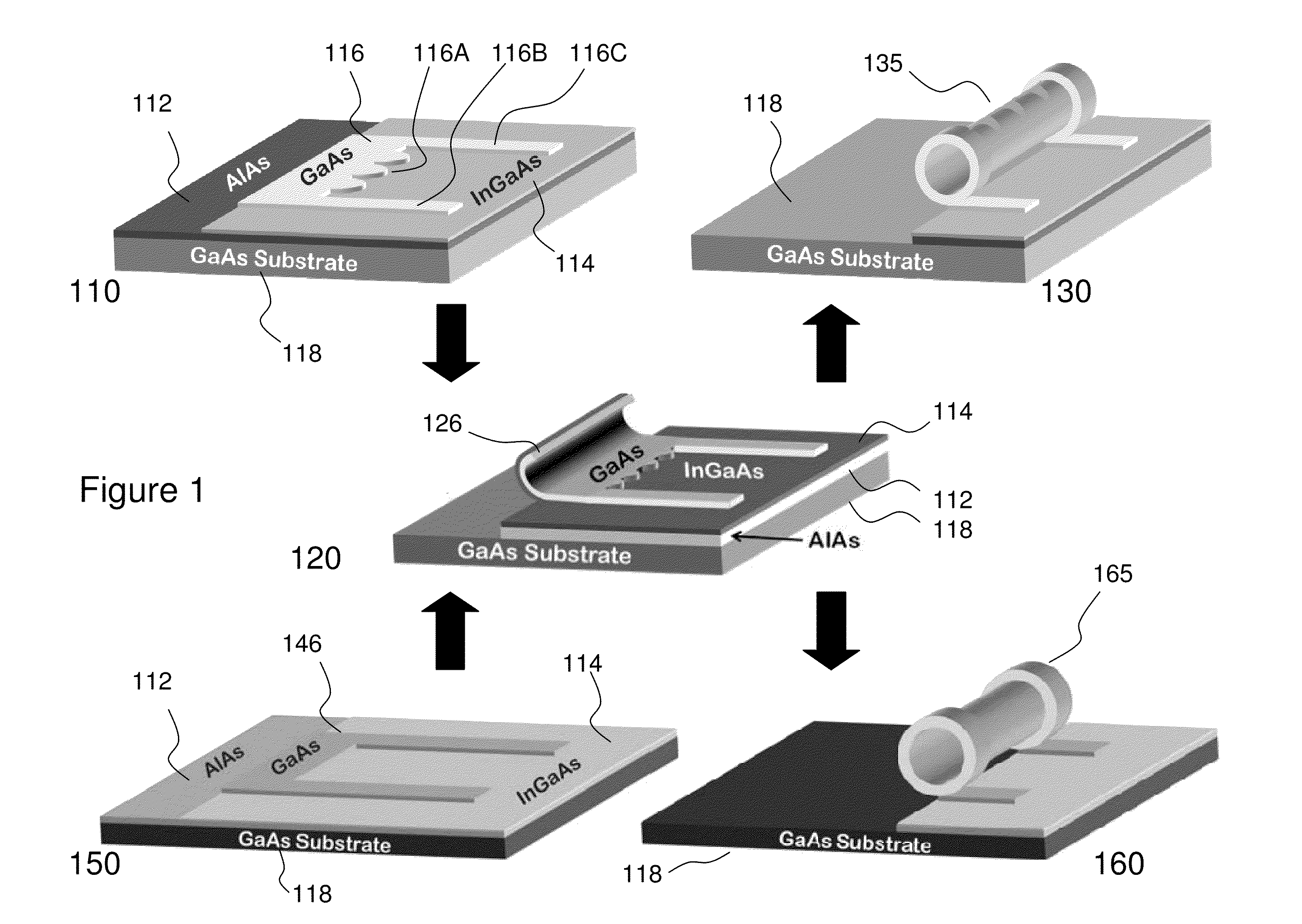
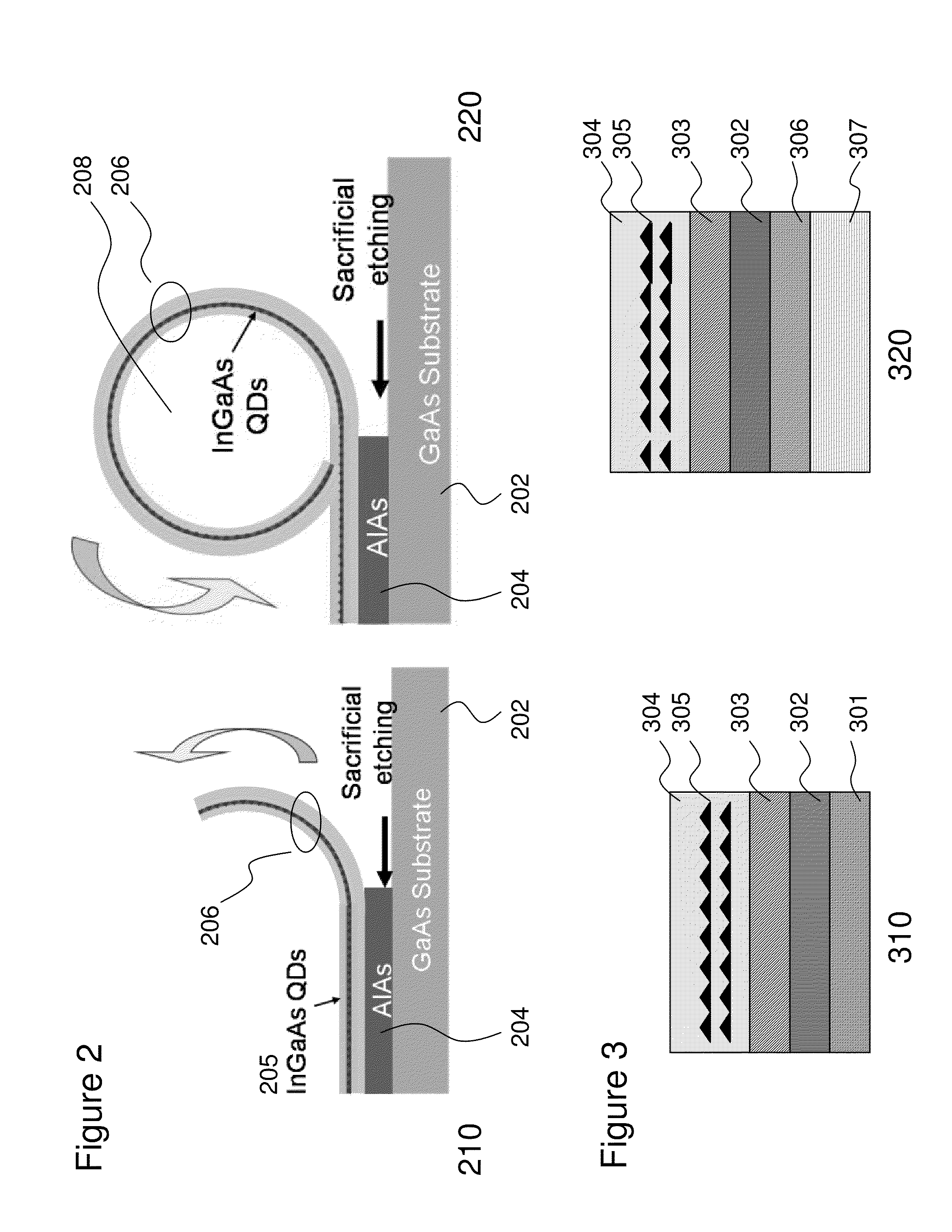
The present invention is directed to semiconductor optical devices, and more specifically to method of manufacturing micro- and nanotubes and devices incorporating them.

Reference may be made below to specific elements, numbered in accordance with the attached figures. The discussion below should be taken to be exemplary in nature, and not as limiting of the scope of the present invention. The scope of the present invention is defined in the claims, and should not be considered as limited by the implementation details described below, which as one skilled in the art will appreciate, can be modified by replacing elements with equivalent functional elements.

Within the text below and the embodiments of manufacturing, use, etc contained within the term “semiconductor tube” has been used and refers to either a semiconductor tube or a semiconductor nanotube. Similarly whilst reference is made primarily to GaAs / InAlGaAs semiconductors for embodiments of the invention it would be understood ...


PUM

PropertyMeasurementUnit
thicknessesaaaaaaaaaa
diametersaaaaaaaaaa

Abstract

Semiconductor micro- and nanotubes allow the incorporation of ordered structures such as quantum wells and quantum dots into them providing the potential for ultralow threshold micro- and nanoscale lasers for use in applications such as future ultrahigh-speed photonic systems as well as quantum information processing. According to the invention a means of manufacturing these with high reproducibility, low processing complexity, and at high densities is provided. Also provided is a means of releasing these micro- and nanotubes with low stress and a method of “pick-and-place” allowing micro- and nanotubes to be exploited in devices integrated on substrates that are either incompatible with the manufacturing technique or where the area of substrate required to manufacture them is detrimental to the cost or performance of the circuit.

Description

FIELD OF THE INVENTIONThis invention relates to semiconductor optical devices, and more specifically to method of manufacturing micro- and nanotubes and devices incorporating them.BACKGROUND OF THE INVENTIONThe development of ultralow threshold micro- and nanoscale lasers is of critical importance for applications in future ultrahigh-speed photonic systems as well as quantum information processing. In fact, a critical yet missing technology for future chip-level optical communications is a high performance and highly reliable laser on silicon. In this regard, III-V semiconductor lasers on Si as well as the monolithic integration with Si-based waveguide devices have been extensively investigated. However, their practical applications have been limited, to a large extent, by the generation and propagation of dislocations, due to the large lattice and thermal mismatches between III-V materials and Si.Accordingly, research has focused to reducing the dimensions of the optical devices to...

Claims


Application Information

Patent Timeline
Patent Type & Authority Applications(United States)
IPC IPC(8): H01L29/06H01L21/302B82Y20/00
CPCB82Y10/00H01L29/06B82Y40/00G02B6/12H01L29/0665H01L29/0673H01L29/66469H01L29/775H01S5/021H01S5/0215H01S5/0217H01S5/1042H01S5/1071H01S5/3412B82Y99/00B82Y20/00
Inventor MI, ZETIAN
Owner MCGILL UNIV
Why Eureka
Try Eureka