Laser diode with ridge waveguide structure and method for manufacturing the same

a laser diode and ridge waveguide technology, applied in the direction of lasers, laser optical resonator construction, laser details, etc., can solve the problems of inferior heat dissipation function of thicker burying layer, inferior thermal conductivity of about 0.3 w/m/k, and use of reinforcing resin, so as to improve the heat dissipation function

Inactive Publication Date: 2011-07-07
SUMITOMO ELECTRIC IND LTD
View PDF1 Cites 20 Cited by
  • Summary
  • Abstract
  • Description
  • Claims
  • Application Information

AI Technical Summary

Benefits of technology

[0007]The arrangement of the LD according to the present invention may enhance the heat dissipating function in the edge reg...

Problems solved by technology

However, when the burying layer is made of resin, the resin used therein has inferior thermal conductivity of about 0.3 W/m/K quite lesser than those of semiconductor materials; accordingly, a thicker bu...

Method used


Image

  • Laser diode with ridge waveguide structure and method for manufacturing the same
  • Laser diode with ridge waveguide structure and method for manufacturing the same
  • Laser diode with ridge waveguide structure and method for manufacturing the same

Examples


first embodiment

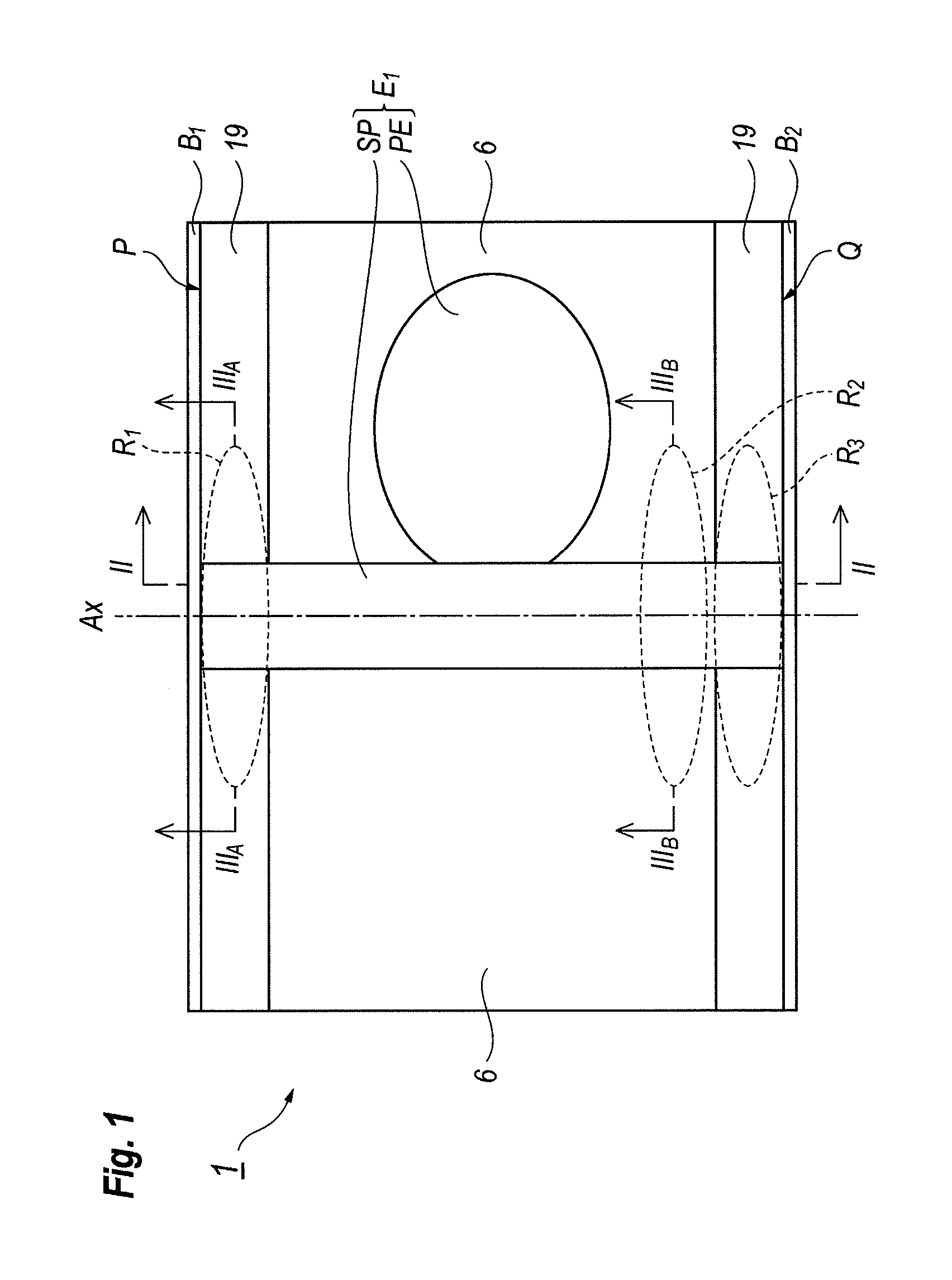
[0030]An LD with the ridge waveguide structure according to an embodiment of the present invention will be described as referring to FIGS. 1 to 3. FIG. 1 is a plan view of the LD 1 with the ridge waveguide structure. The LD 1 provides no resin layer 6 in edge regions of the device. Edge regions close to one facet P and to the other facet Q of the LD 1 has no resin layer 6; accordingly, an insulating layer 19 exposes thereat. The stripe SP of the first electrode E1, which provides an upper electrode of the LD 1, extends from the facet P to the other facet Q along the axis Ax. In the present embodiment, the axis Ax corresponds to a direction along which the light is guided.

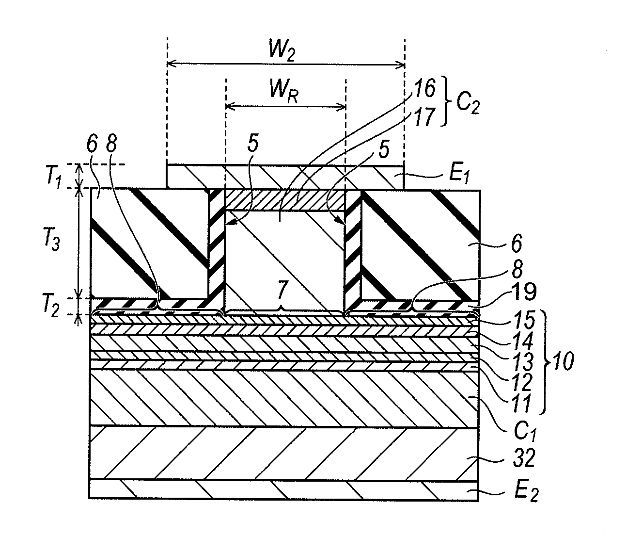
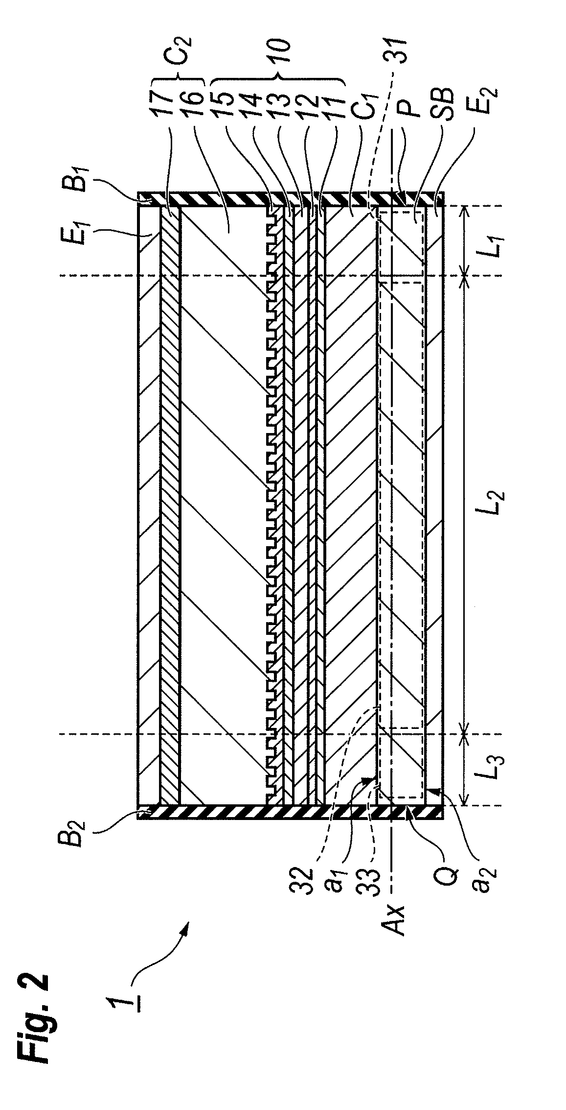
[0031]FIG. 2 is a cross section taken along the line II-II appeared in FIG. 1. As shown in FIG. 2, the LD 1 with the ridge waveguide structure comprises a semiconductor substrate SB, a lower cladding layer C1, a core region 10, a ridge waveguide C2, the first electrode E1 and the second Electrode E2. The semiconduct...

second embodiment

[0070]Next, a second embodiment according to the present invention will be described as referring to FIGS. 16 and 17. FIG. 16 is a plan view showing an LD 2 with the ridge waveguide structure, while, FIGS. 17A and 17B are cross sections of the edge region taken along the line XVIA-XVIA, and along the line XVIB-XVIB, respectively.

[0071]The LD 2 with the ridge waveguide structure of the second embodiment has a feature distinguishable from the first embodiment is that a width of striped portion SP of the first electrode E1 is narrowed in the edge regions, 31 and 33. When the operational speed of the LD reaches and sometimes exceeds 10 Gbit / sec, it is preferable to decrease the capacitance, not only the junction capacitance but the parasitic capacitance, as small as possible. The LD 2 according to the second embodiment provides the first electrode E1 with a narrowed stripe SP in the edge regions, 31 and 33.

[0072]As shown in FIGS. 16 and 17, the first electrode E1 provides the striped po...


PUM


Abstract

An LD with an improved heat dissipating function in the edge regions is disclosed. The LD provides the core region including the active layer and extending whole of the substrate, and the ridge waveguide structure on the core region that extends in a direction along which the light generated in the active layer is guided. The ridge waveguide structure is buried by a thick resin layer in both sides thereof, but the resin layer is removed in the edge regions close to respective facets of the LD.

Description

BACKGROUND OF THE INVENTION[0001]1. Field of the Invention[0002]The present invention relates to a semiconductor laser diode (hereafter denoted as LD) with a ridge waveguide structure, and a method to manufacture the LD.[0003]2. Related Prior Art[0004]In an LD with the ridge waveguide structure, the active layer accompanied with optical confinement layers extends in a plane, but a waveguide with a striped structure extending in one direction within the plane is formed above the laterally extending active layer, and the ridge waveguide made of semiconductor materials is buried with the burying layer. The United States Patent published as US 20090141764A or Aoki et al. in IEEE Quantum Electronics, vol. QE-3(2), (1997), pp. 672 have disclosed one type of the LD with the ridge waveguide structure with a burying layer made of resin. This resin layer extends from one facet of the LD to the other facet. In such an LD, semiconductor materials including the burying layer to bury the ridge wa...

Claims


Application Information

Patent Timeline
IPC IPC(8): H01S5/22H01L21/56H01S5/12
CPCH01S5/02461H01S5/0425H01S5/12H01S5/2009H01S2301/176H01S5/22H01S5/2213H01S5/2231H01S5/2081H01S5/04254
Inventor ONISHI, YUTAKAYAGI, HIDEKI
Owner SUMITOMO ELECTRIC IND LTD
Why Eureka
Try Eureka