Method of forming power mosfet

a technology of power mosfet and field effect transistor, which is applied in the direction of basic electric elements, electrical apparatus, and semiconductor devices, can solve the problems of affecting the working affecting the efficiency of power mosfet, and categorized into switching losses. achieve the effect of lowering the gate-to-drain capacitan

Active Publication Date: 2011-07-14
EXCELLIANCE MOS
View PDF3 Cites 2 Cited by
  • Summary
  • Abstract
  • Description
  • Claims
  • Application Information

AI Technical Summary

Benefits of technology

Accordingly, the invention is directed to a method of forming a power MOSFET. This method adopts a trimming process and a self-aligned process to p...

Problems solved by technology

Therefore, misalignments between contact plugs and trenches in power MOSFETs easily occur so as to affect the performance of the device.
For example, misalignments between contact plugs and trenches affect the variat...

Method used


Image

  • Method of forming power mosfet
  • Method of forming power mosfet
  • Method of forming power mosfet

Examples


Embodiment Construction

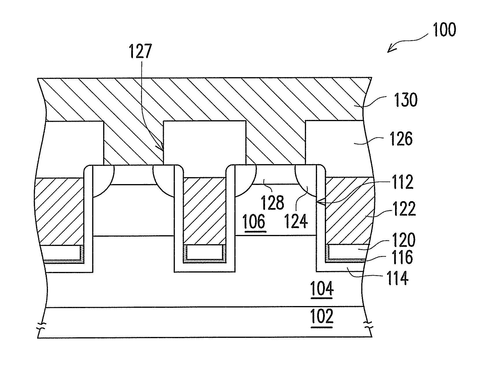
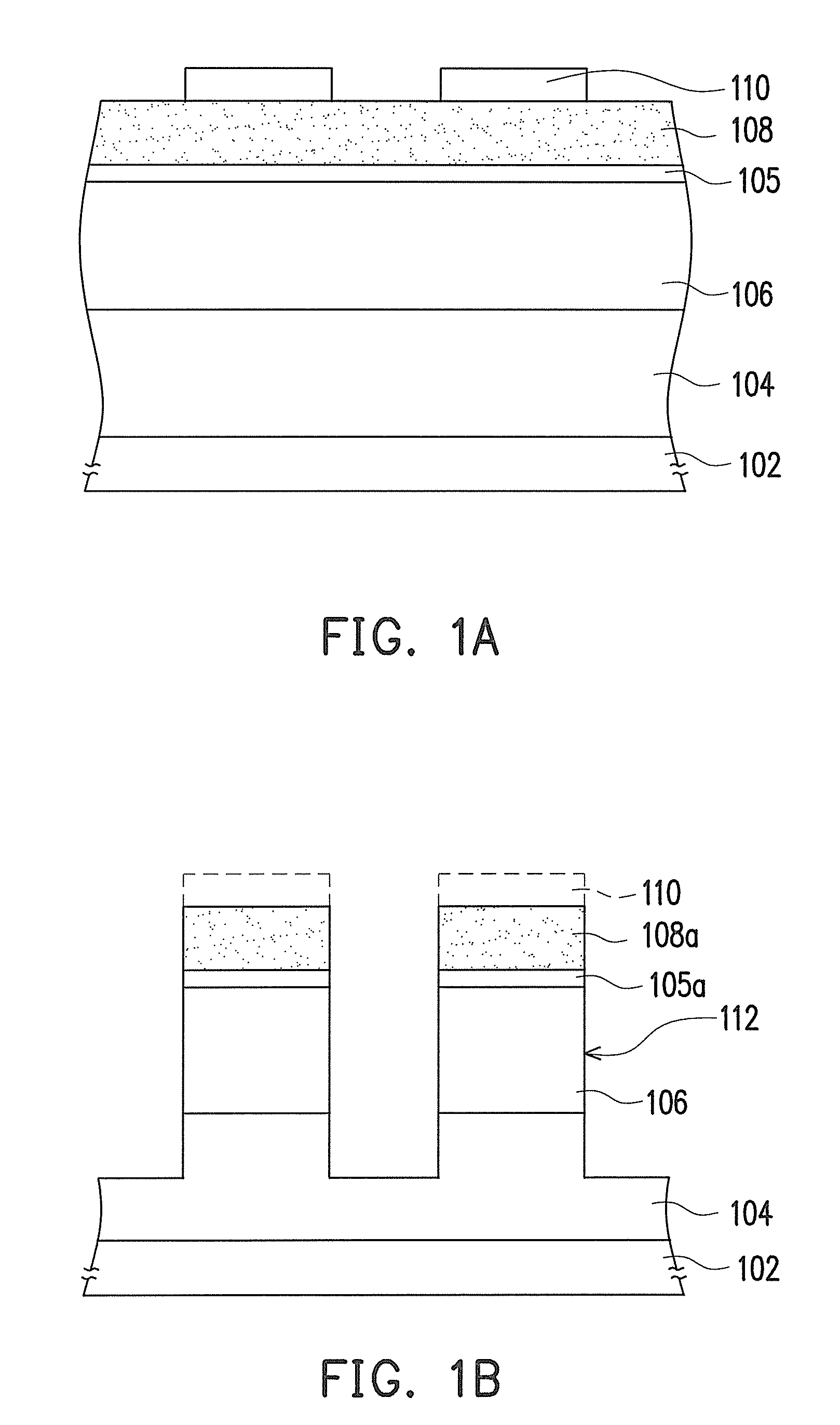
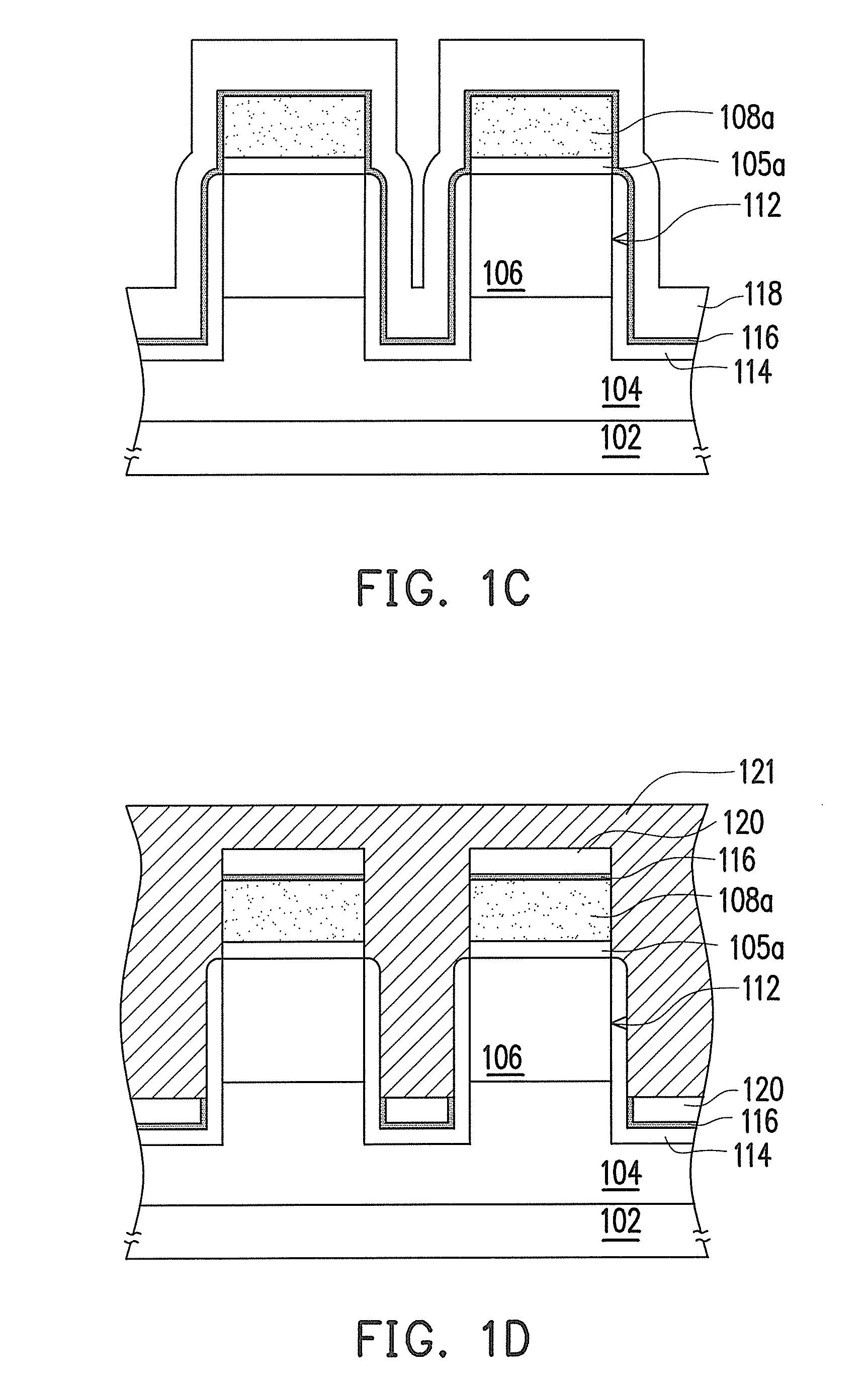
FIGS. 1A through 1H are cross-sectional views schematically depicting a method of forming a power MOSFET according to an embodiment of the invention.

Referring to FIG. 1A, an epitaxial layer 104 of a first conductivity type is formed on a substrate 102 of the first conductivity type. Here, the substrate 102 of the first conductivity type serves as a drain. The substrate 102 is, for example, an N-type heavily-doped silicon substrate. The epitaxial layer 104 is, for example, an N-type lightly-doped epitaxial layer, and the formation method thereof includes performing a selective epitaxy growth (SEG) process. A body layer 106 of a second conductivity type is then formed in the epitaxial layer 104. The body layer 106 is, for example, a P-type body layer, and the formation method thereof includes performing an ion implantation process and a subsequent drive-in process. In one embodiment of the invention, after the step of forming the epitaxial layer 104 and before the step of forming the ...


PUM


Abstract

A method of forming a power MOSFET is described. An epitaxial layer of first conductivity type is formed on a substrate of first conductivity type. A body layer of second conductivity type is formed in the epitaxial layer. A plurality of mask patterns are formed on the substrate. A plurality of trenches are formed in the body layer and the epitaxial layer between the mask patterns. An oxide layer is formed on surfaces of the trenches. A conductive layer is formed in the trenches. A trimming process is performed to the mask patterns to reduce the line width of each mask pattern. Two source regions of first conductivity type are formed in the body layer beside each trench by using the trimmed mask patterns as a mask. A plurality of dielectric patterns are formed on the conductive layer and between the trimmed mask patterns. The trimmed mask patterns are removed.

Description

BACKGROUND OF THE INVENTION1. Field of the InventionThe invention relates to a method of forming a semiconductor device, and more particularly, to a method of forming a power metal-oxide-semiconductor field effect transistor (MOSFET).2. Description of Related ArtPower MOSFETs are widely applied to power switching devices, for example, power supplies, converters, or low-voltage motor controller, and the like. In general, a conventional power MOSFET adopts a vertical structural design to enhance the device density. For each power MOSFET, each drain region is formed on the back-side of a chip, and each source region and each gate are formed on the front-side of the chip. The drain regions of the transistors are connected in parallel so as to endure a considerable large current.As the level of integration of power MOSFETs increases, the dimension of the same is reduced as well. Therefore, misalignments between contact plugs and trenches in power MOSFETs easily occur so as to affect the ...

Claims


Application Information

Patent Timeline
IPC IPC(8): H01L21/336
CPCH01L29/42368H01L29/511H01L29/7813H01L29/66734H01L29/518
Inventor CHANG, YI-CHIWU, CHIA-LIEN
Owner EXCELLIANCE MOS
Why Eureka
Try Eureka