Optical modulator and optical modulator fabrication method

Inactive Publication Date: 2011-07-21
NEC CORP
View PDF1 Cites 51 Cited by
  • Summary
  • Abstract
  • Description
  • Claims
  • Application Information

AI Technical Summary

Benefits of technology

Although optical phase modulation is possible in the method of Patent Document 1, the thickness of regions in which the carrier density changes dynamically is extremely thin, i.e., in the order of several tens of nm. As a result, an optical modulation length in the millimeter order (1 mm or more) becomes necessary, the size of the optical modulator increases, and high-speed operation becomes problematic. Accordin

Problems solved by technology

As a result, an optical modulation length in the millimeter order (1 mm or more) becomes necessary, the size of the optical modulator increases, and high-speed operation becomes problematic.
Accordingly, regarding silicon-base optical modulators that can be integrated on a silicon substrate, it is difficult

Method used


Image

  • Optical modulator and optical modulator fabrication method
  • Optical modulator and optical modulator fabrication method
  • Optical modulator and optical modulator fabrication method

Examples


Example

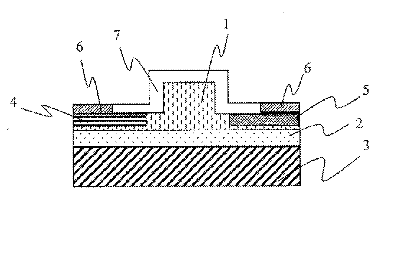
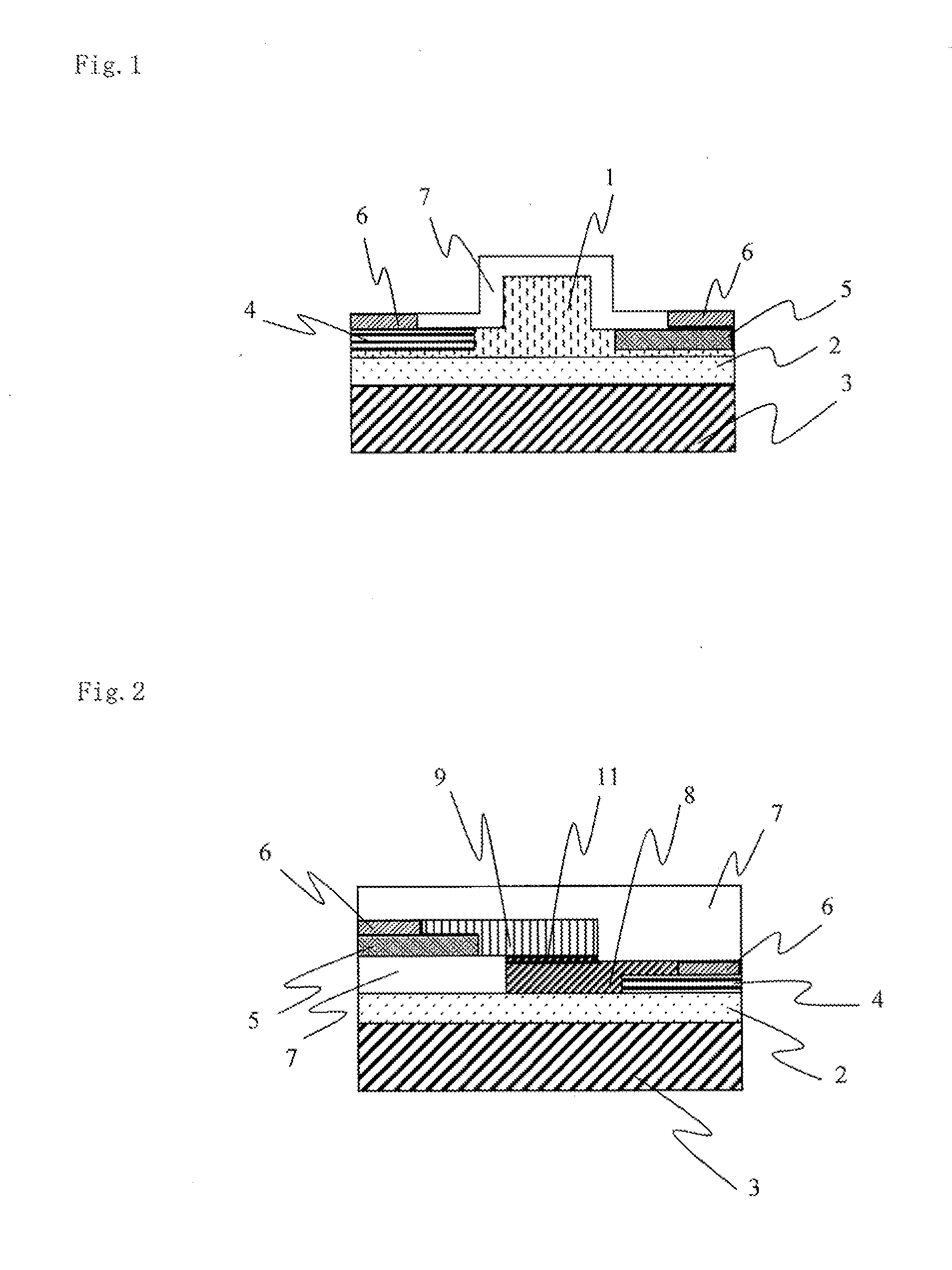
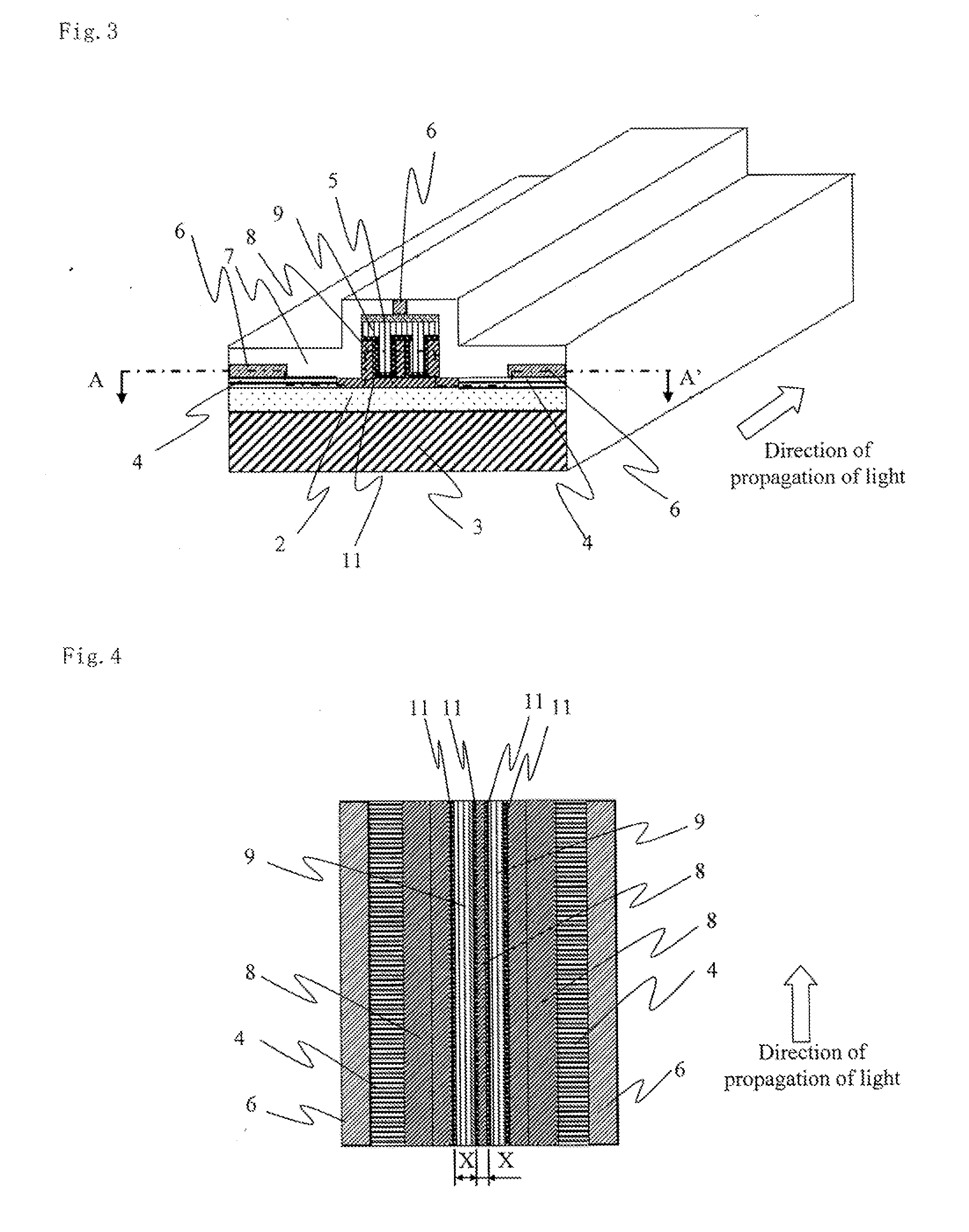
Exemplary embodiments of the present invention are next described based on the accompanying drawings. Constructions having identical functions are given the same numbers in the accompanying drawings and redundant explanation of these constructions may be omitted.

Before describing a typical construction of the optical modulator of the present invention, the mechanism of modulation of the carrier density within a silicon layer, which is the basis of the operation of the present invention, will first be explained. The silicon-base optical modulator of the present invention uses the carrier plasma effect that is next described.

As previously described, pure silicon does not exhibit change of the index of refraction due to the Pockels effect, and changes in the index of refraction due to the Franz-Keldysh effect or Kerr effect are extremely small. As a result, only the carrier plasma effect and thermo-optic effect can be used in optical modulation operations. However, an optical modulator...


PUM


Abstract

An optical modulator is formed with at least a portion of a semiconductor layer (8) that has undergone a doping process to exhibit a first conductivity and at least a portion of a semiconductor layer (9) that has undergone a doping process to exhibit a second conductivity overlapping with a dielectric layer (11) interposed. The surface of the semiconductor layer (8) of first conductivity has an uneven form in the portion in which the semiconductor layer (8) that exhibits first conductivity and the semiconductor layer (9) that exhibits second conductivity overlap with the dielectric layer (11) interposed. The dielectric layer (11) is formed on the semiconductor layer (8) of first conductivity that has the uneven form, and the semiconductor layer (9) of second conductivity is formed on the dielectric layer (11).

Description

TECHNICAL FIELDThe present invention relates to an optical modulator that is necessary in the information processing and communication fields and that converts high-speed electrical signals to optical signals at high speed and to a fabrication method of the optical modulator; and more particularly, relates to an optical modulator that uses a capacitor construction composed of silicon-insulator-silicon that is formed on an SOI (Silicon on Insulator) substrate and to a fabrication method of the optical modulator.BACKGROUND ARTOptical fiber communication that was chiefly used for business has now come to be widely used in repidences. This popularization has been accompanied by a demand for high-performance optical communication devices. Among the various optical communication devices for optical communication systems such as local area networks (LAN) and optical fiber for residential use are included silicon-base optical communication devices that function at the optical signal wavelen...

Claims


Application Information

Patent Timeline
IPC IPC(8): G02F1/025B05D5/12
CPCG02F2001/0152G02F1/025G02F1/0152
Inventor FUJIKATA, JUNICHIBABA, TOSHIOUSHIDA, JUN
Owner NEC CORP
Why Eureka
Try Eureka