This helps you quickly interpret patents by identifying the three key elements:
Problems solved by technology
Method used
Benefits of technology
Benefits of technology
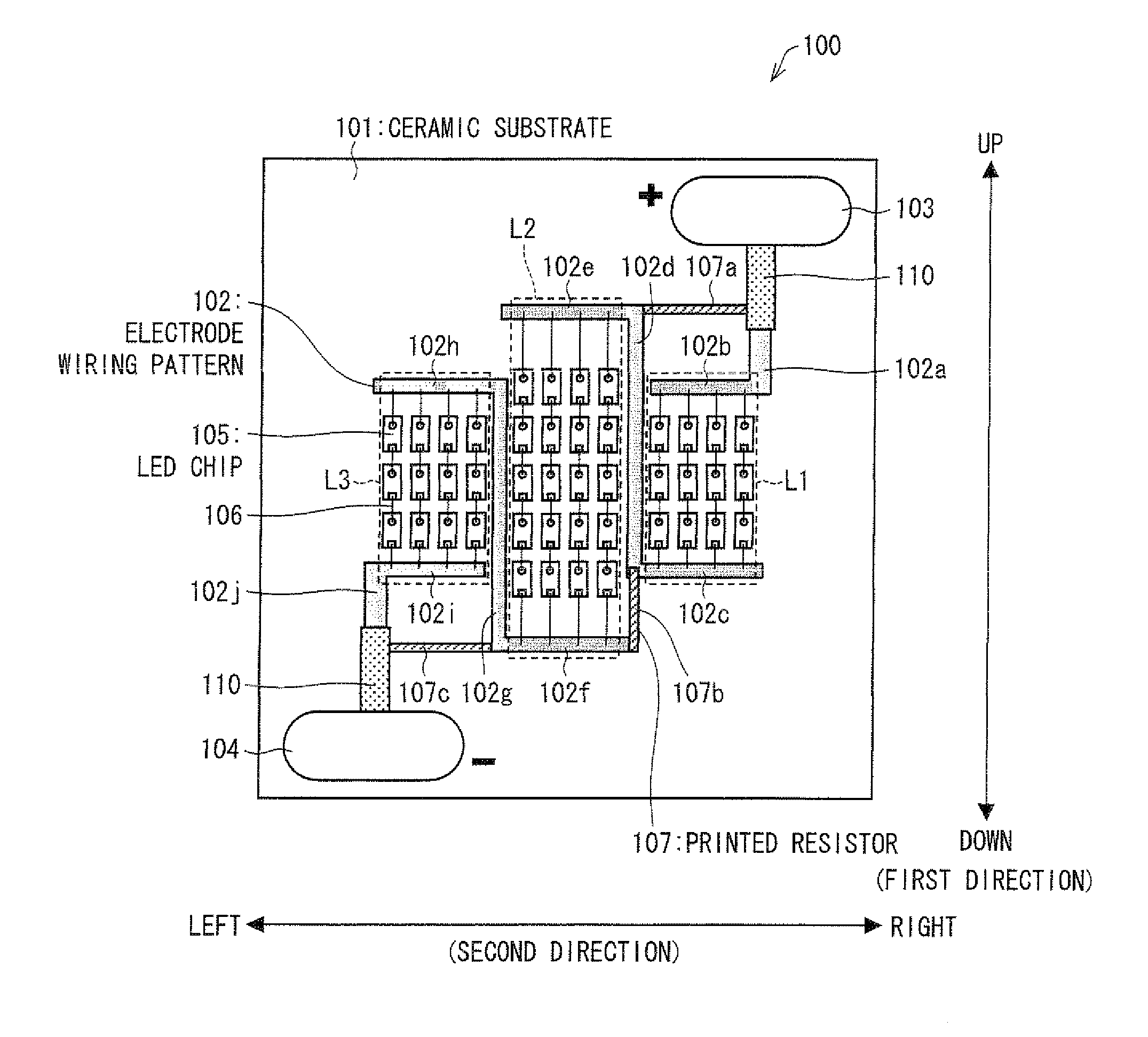
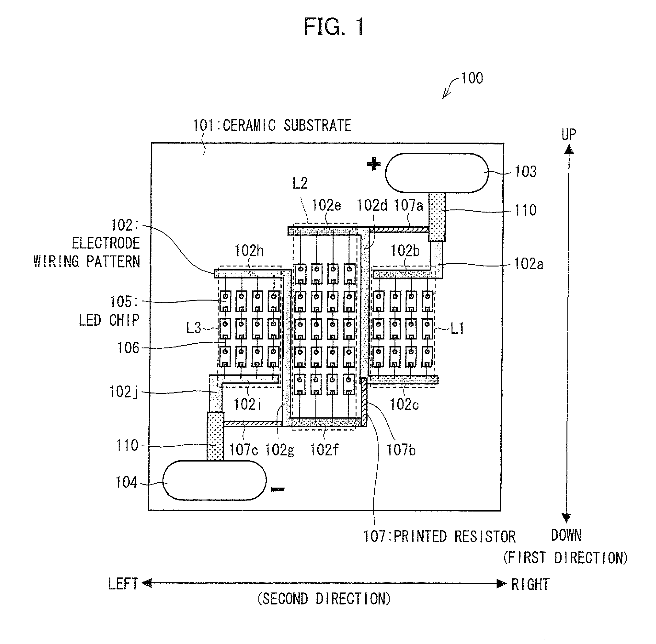
[0026]As described above, the light emitting device of the present invention includes: a substrate; a plurality of light emitting elements provided on a primary surface of the substrate; at least one protective element connected in parallel with the plurality of light emitting element; a resin frame made of a resin having a low optical transmittance, the resin frame being provided annularly on the primary surface of the substrate so as to surround a mounting area in which the plurality of light emitting elements are provided; a fluorescent-material-containing resin layer made of a resin containing fluorescent materials, the fluorescent-material-containing resin layer being provided adjacent to an inner side of the resin frame so as to cover the plurality of light emitting elements; and at least one first light emitting element connection electrode and at least one second light emitting element connection electrode, which are provided on the primary surface of the substrate so as to face each other along a first direction in the primary surface. The light emitting device of the present invention is configured such that (i) the plurality of light emitting elements has such a circuit configuration that at least two series circuit sections, in each of which at least two of the plurality of light emitting elements are connected in series, are connected in parallel between the at least one first light emitting element connection electrode and the at least one second light emitting element connection electrode, (ii) the at least two series circuit sections are aligned along a second direction orthogonal to the first direction in the primary surface, between the at least one first light emitting element connection electrode and the at least one second light emitting element connection electrode, (iii) the at least two of the plurality of light emitting elements in each of the at least two series circuit sections are aligned along the first direction, and (iv) the at least one first light emitting element connection electrode and the at least one second light emitting element connection electrode are disposed below at least one of the resin frame and the fluorescent-material-containing resin layer.
[0027]In the above configuration, the first light emitting element connection electrode and the second light emitting element connection electrode are disposed so as to sandwich a mounting area where the light emitting elements are provided. Further, the light emitting elements in a series circuit section are directly wire-bonded, for example, so as to be electrically connected to each other. Accordingly, it is unnecessary to provide conventionally used electrode wiring patterns. This configuration reduces distances between the light emitting elements, thereby increasing a packaging density of the light emitting elements. Consequently, it is advantageously possible to restrain that light emitted from the light emitting elements appears bright dots and to restrain in-plane luminance unevenness of the light emitting device. Furthermore, it is also advantageously possible to downsize the light emitting device.
[0028]Further, when largest possible parts of the first light emitting element connection electrode and the second light emitting element connection electrode are disposed below the resin frame, light absorption by these electrodes can be restrained. In addition to this, light absorption by the electrode wiring patterns is also reduced. This accordingly makes it possible to improve the luminous efficiency. Further, since the protective element is connected in parallel with the light emitting elements, it is possible to prevent deterioration of the light emitting elements, thereby allowing the light emitting device to be used for a longer term and ensuring its reliability. As a result, it is possible to provide a light emitting device having excellent luminous efficiency and excellent reliability.
Problems solved by technology
However, LEDs, especially, galliumnitride LEDs are easily broken due to electrostatic discharges.
In such a configuration that employs the Zener diodes, when an excessive voltage is applied in a forward direction, an excessive current is bypassed due to Zener breakdown.
This arises such a problem that the current flowing through the bypass resistor causes large energy loss.
The semiconductor light emitting device also has such a problem that large energy loss occurs because an electric resistance of the variable resistors should be low.
Method used
Image
Click on the blue label to locate the original text in one second.
Reading with bidirectional positioning of images and text.
Examples
embodiment 1
[0044]The following describes one embodiment of the present invention with reference to drawings. Initially explained is an entire configuration of a light emitting device, briefly. Then, characteristic configurations, a production method, and the like of the light emitting device will be explained in order.
[0045](Entire Configuration)
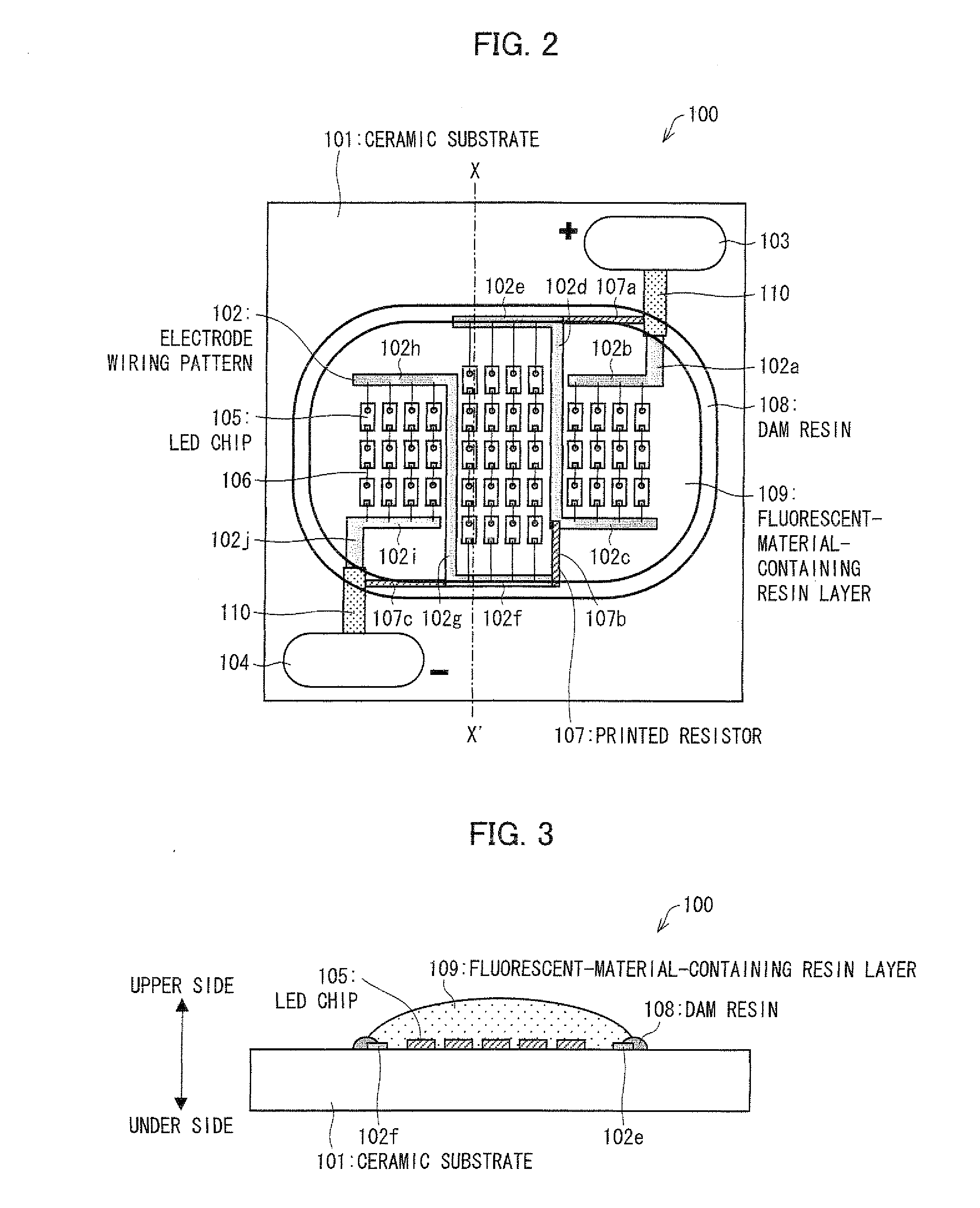
[0046]FIG. 1 is a top view illustrating one exemplary configuration of a light emitting device 100 according to the present embodiment. More specifically, FIG. 1 illustrates the light emitting device 100 in which LED chips 105 and the like are provided on a primary surface of a ceramic substrate 101 but they have not been resin-molded yet. FIG. 2 is a top view illustrating one exemplary configuration of the light emitting device 100 of the present embodiment. More specifically, FIG. 2 illustrates the light emitting device 100 as a finished package in which the LED chips 105 and the like provided on the primary surface of the ceramic substrate 101 are r...
modified example
[0121]The aforementioned light emitting device 100 uses a ceramic substrate 101, but is not limited to this. The light emitting device 100 may use other substrates instead. For example, a metal core substrate including a metal substrate on whose surface an insulating layer is provided may be used. In this case, the insulating layer is formed only in an area where the printed resistors 107 and the electrode wiring pattern 102 are to be formed, so that a plurality of LED chips 105 are directly provided on the metalsubstrate surface.
[0122]Further, the outer shape of the ceramic substrate 101 is not limited to a rectangular shape. Further, the vertical direction (up-and-down direction / first direction) and the horizontal direction (left-to-right direction / second direction) on the primary surface is not determined based on the outer shape of the primary surface, but is determined depending on relative positional relationship of the electrode wiring pattern 102, the LED chips 105, and the...
embodiment 2
[0127]FIG. 5 is a top view illustrating one exemplary configuration of a light emitting device 200 of the present embodiment.
[0128]The light emitting device 200 of the present embodiment is different from the light emitting device 100 of Embodiment 1 in terms of how the electric circuit is configured. Except for this point, the light emitting device 200 has a configuration equivalent of the light emitting device 100 of Embodiment 1.
[0129]As illustrated in FIG. 5, the light emitting device 200 has a circuit configuration in which 14 series circuit sections, in each of which 7 LED chips 105 are linearly aligned so as to be connected in series, are connected in parallel. In other words, 98 LED chips 105 in total, which are connected in a series-parallel connection (i.e., 7-series-connected LED chips per series circuit section×14 parallel-connected series circuit sections), are provided on a primary surface of a ceramic substrate 101.
[0130]The electrode wiring pattern 102 is constituted...
PUM
Abstract
A light emitting device includes: a ceramic substrate; a plurality of LED chips; a printed resistor(s) connected in parallel with the plurality of LED chips; a dam resin made of a resin having a low optical transmittance; a fluorescent-material-containing resin layer; and an anode-side electrode and a cathode-side electrode, (a) which are provided on a primary surface of the ceramic substrate so as to face each other along a first direction on the primary surface and (b) which are disposed below at least one of the dam resin and the fluorescent-material-containing resin layer. With the configuration in which a plurality of LEDs, which are connected in a series-parallel connection, are provided on a substrate, it is possible to provide a light emitting device which can achieve restraining of luminance unevenness and an improvement in luminous efficiency.
Description
[0001]This Nonprovisional application claims priority under 35 U.S.C. §119(a) on Patent Application No. 2010-012486 filed in Japan on Jan. 22, 2010, the entire contents of which are hereby incorporated by reference.TECHNICAL FIELD[0002]The present invention relates to a light emitting device including a plurality of light emitting elements provided in a series-parallel connection, and a protective element(s), which is electrically connected to the plurality of light emitting elements. Particularly, the present invention relates to a technique to restrain luminance unevenness and to improve luminous efficiency.BACKGROUND ART[0003]As an improvement in luminous efficiency becomes more important in recent years, LEDs (Light Emitting Diode) are being widely used in backlights provided in a display device and lighting apparatuses as a light source that saves more energy than electric bulbs or fluorescent lamps. For these purposes, energy efficiency is very important.[0004]However, LEDs, e...
Claims
Application Information
Patent Timeline
Application Date:The date an application was filed.
Publication Date:The date a patent or application was officially published.
First Publication Date:The earliest publication date of a patent with the same application number.
Issue Date:Publication date of the patent grant document.
PCT Entry Date:The Entry date of PCT National Phase.
Estimated Expiry Date:The statutory expiry date of a patent right according to the Patent Law, and it is the longest term of protection that the patent right can achieve without the termination of the patent right due to other reasons(Term extension factor has been taken into account ).
Invalid Date:Actual expiry date is based on effective date or publication date of legal transaction data of invalid patent.

