Electronic device and method of manufacturing the same

a technology of electronic devices and manufacturing methods, applied in the direction of solid-state devices, film/foil adhesives, basic electric elements, etc., can solve the problems of defective sealing, defective bonding connection, and various drawbacks, and achieve the effect of reducing the emission rate of siloxane gas during the heating of silicone adhesives and sufficiently reducing the emission rate of siloxane gas

Inactive Publication Date: 2011-07-28
DENSO CORP +1
View PDF5 Cites 6 Cited by
  • Summary
  • Abstract
  • Description
  • Claims
  • Application Information

AI Technical Summary

Benefits of technology

[0010]In the electronic device using the silicone adhesive made from the above composition, the emission rate of siloxane gas during the heating of the silicone adhesive is sufficiently reduced.
[0011]The electronic device having the above silicone adhesive is manufactured by placing the first member and the second member on top of each other through the composition, and heating the composition in one of a vacuum environment and an evacuation environment. In such a method, in addition to the effect of reducing the emission rate of the siloxane gas, it is less likely that the siloxane gas will adhere to surfaces of parts on one of the first member and the second member.

Problems solved by technology

Therefore, various drawbacks, such as defective sealing, defective bonding connection, defective connection of the electrically conducive paste, are likely to occur due to siloxane gas generated when the silicone adhesive is heated for curing.
However, even if such siloxane compositions having the reduced content of low molecular weight siloxane are used for the adhesive of the electronic device, it is difficult to sufficiently reduce the above drawbacks.

Method used


Image

  • Electronic device and method of manufacturing the same
  • Electronic device and method of manufacturing the same
  • Electronic device and method of manufacturing the same

Examples


first embodiment

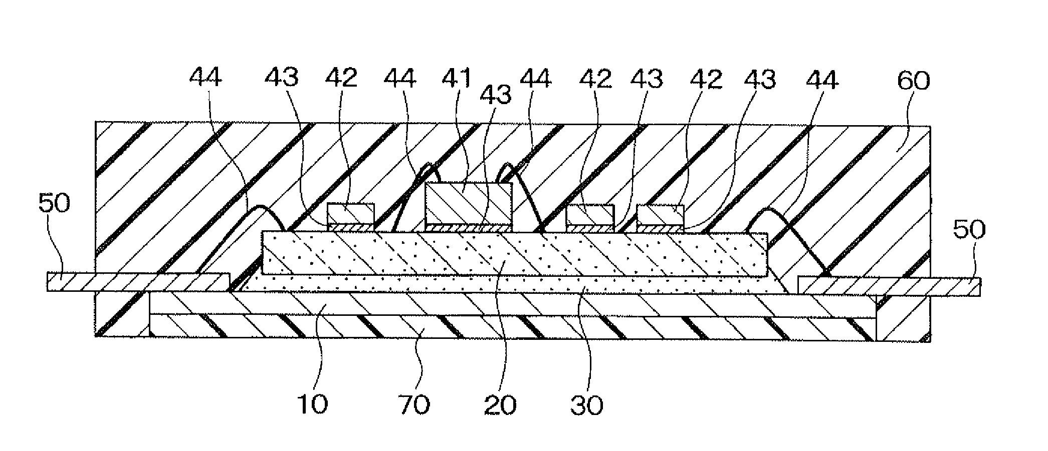
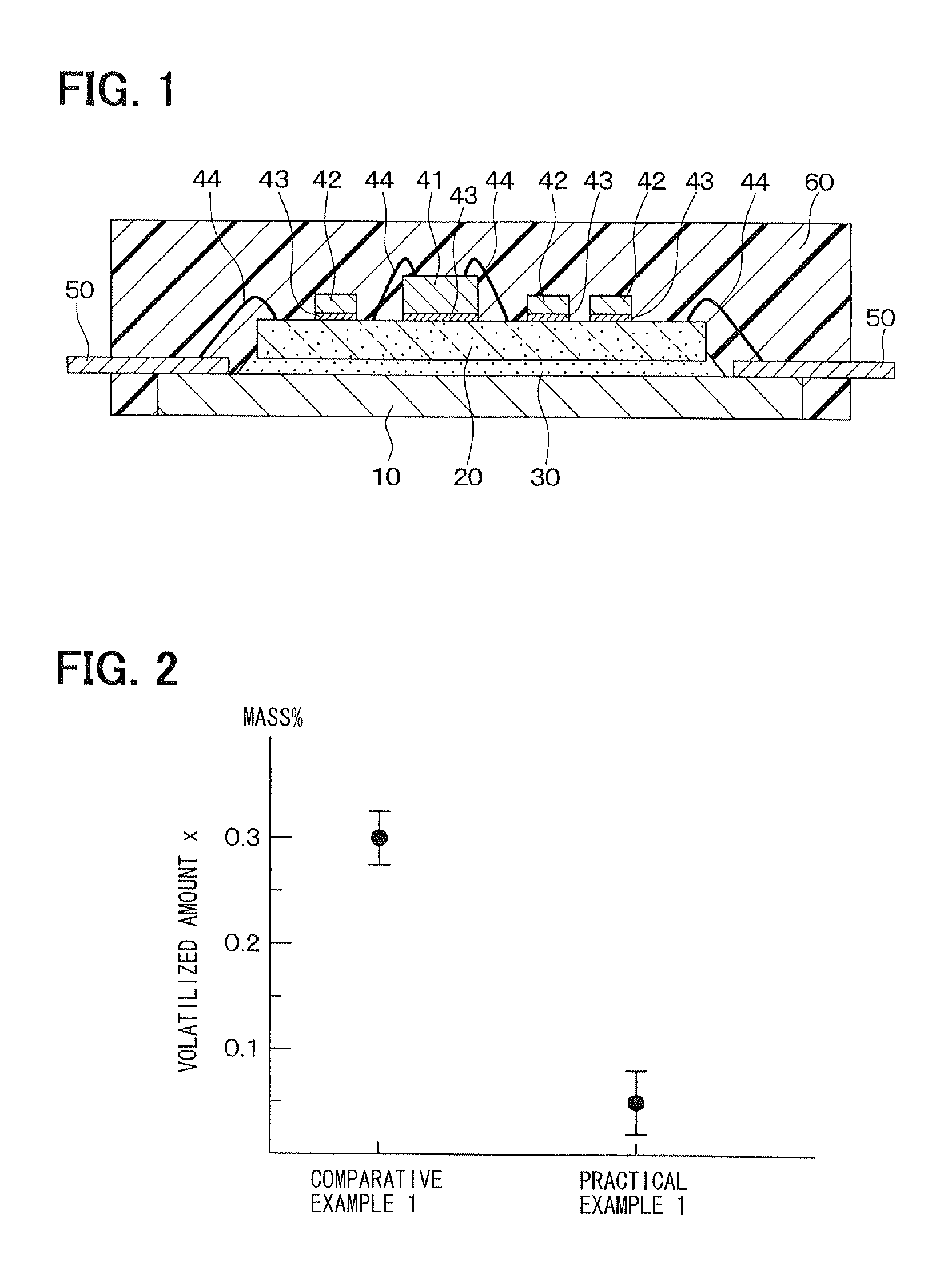
[0019]Referring to FIG. 1, in an electronic device according to the first embodiment, a substrate 20 is mounted on a surface, such as a top surface in FIG. 1, of a heat sink 10 through a silicone adhesive 30.

[0020]The heat sink 10, which is for example constituted as a first member, is a plate member having heat radiation performance. A material of the heat sink 10 is optimally selected, such as from Fe, Al, Cu, a Cu-Mo alloy, and an Al-SiC complex. In a case where the heat sink 10 is made of Fe, the surfaces thereof may be plated with Ni.

[0021]The substrate 20 is a common circuit board, and is for example constituted as a second member. The substrate 20 has a plate shape having a front surface, such as a top surface in FIG. 1, and a rear surface, such as a bottom surface in FIG. 1.

[0022]The silicone adhesive 30 is disposed along the rear surface of the substrate 20 to bond the rear surface to the heat sink 10. The substrate 20 is optimally selected, such as from an alumina substrat...

second embodiment

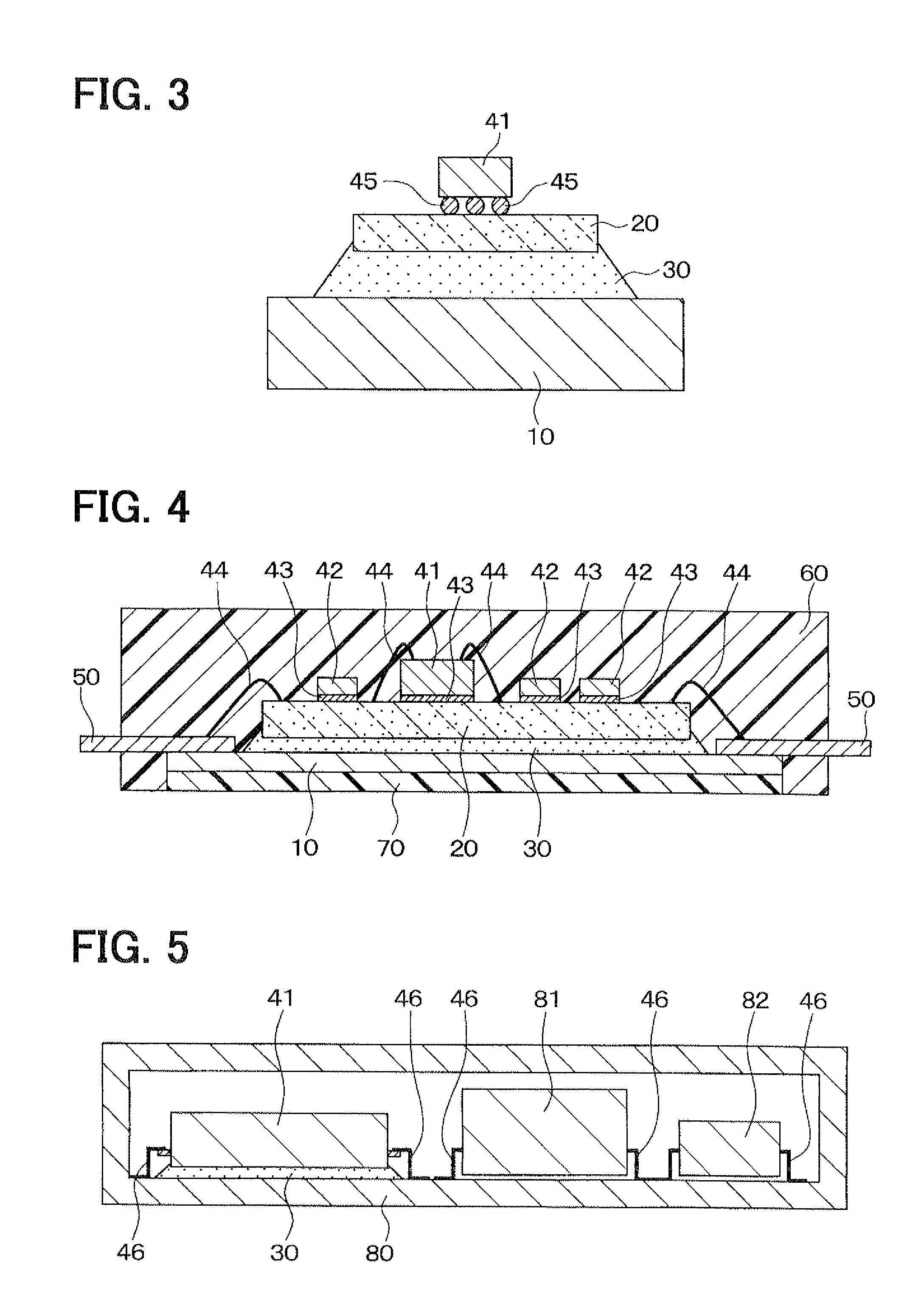
[0084]FIG. 3 shows a main part of an electronic device according to a second embodiment. A main difference of the electronic device of the second embodiment from the electronic device of the first embodiment is that the IC chip 41 is connected to the substrate 20 by flip-chip bonding.

[0085]As shown in FIG. 3, the IC chip 41 is connected to the substrate 20 through bumps 45 made of gold, copper or the like. In a case where the electronic device has a connecting structure of the flip-chip bonding, the silicone adhesive 30 needs to be cured by heating before the flip-chip bonding.

[0086]Also in this case, the aforementioned effect of the silicone adhesive 30 is demonstrated. That is, the emission rate of the siloxane gas is reduced, and thus the adhering of the siloxane gas to the bonding lands is minimized. Therefore, defective bonding connection is reduced. The electronic device having favorable functions can be achieved.

third embodiment

[0087]FIG. 4 shows an electronic device according to a third embodiment. The electronic device shown in FIG. 4 has an insulating radiation sheet 70 along the heat sink 10 provided by a lead frame on a side opposite to the substrate 20. The insulating radiation sheet 70 uses a silicone resin, an epoxy resin or the like, as a main component. Other structures are similar to the electronic device of FIG. 1.


PUM

PropertyMeasurementUnit
mass %aaaaaaaaaa
viscosityaaaaaaaaaa
viscosityaaaaaaaaaa

Abstract

In an electronic device, a silicone adhesive bonding first and second members is made from a composition comprising: (A) 100 parts by mass of an organopolysiloxane containing in one molecule at least two alkenyl groups and being free of silicon-bonded hydroxyl and alkoxy groups wherein the content of cyclic siloxanes having 4 to 20 siloxane units is at most 0.1 mass %; (B) an organopolysiloxane containing in one molecule at least two silicon-bonded hydrogen atoms and being free of an alkenyl group, and silicon-bonded hydroxyl and alkoxy groups; (C) at least 0.05 parts by mass of an adhesion promoter; (D) 100 to 2000 parts by mass of a thermally conductive filler; and (E) a hydrosilylation-reaction catalyst. (B) is contained such that the silicon-bonded hydrogen atoms is in the range of 0.5 to 10 mol per 1 mol of the alkenyl groups of (A), and the sum of (B) and (C) is 0.5 to 10 mass % of the sum of (A), (B) and (C).

Description

CROSS REFERENCE TO RELATED APPLICATION[0001]This application is based on Japanese Patent Application No. 2010-16844 filed on Jan. 28, 2010, the disclosure of which is incorporated herein by reference.FIELD OF THE INVENTION[0002]The present invention relates to an electronic device having a bonding structure using a silicone adhesive and a method of manufacturing the same.BACKGROUND OF THE INVENTION[0003]With regard to such an electronic device, in general, a first member and a second member, such as a circuit board and a heat sink, are bonded to each other by curing a silicone adhesive with heat between the first member and the second member.[0004]On the circuit board, for example, electronic components are connected through an electrically conductive paste and the like, and connecting structures are formed by wire bonding, flip chip bonding and the like. Further, the circuit board and the electronic components are sealed with a mold resin. Therefore, various drawbacks, such as defe...

Claims


Application Information

Patent Timeline
Patent Type & Authority Applications(United States)
IPC IPC(8): H01L23/48H01L21/50
CPCC08G77/04H01L2924/01047C08L83/04H01L23/296H01L23/3121H01L23/36H01L23/4334H01L23/49531H01L24/13H01L24/29H01L24/45H01L24/48H01L2224/13144H01L2224/13147H01L2224/45124H01L2224/45144H01L2224/45147H01L2224/48091H01L2224/48227H01L2224/73265H01L2924/01004H01L2924/01014H01L2924/01046H01L2924/01078H01L2924/01079H01L2924/014H01L2924/0781H01L2924/14H01L2924/19041H01L2924/19105H01L2924/19107C08G77/20H01L2924/01028H01L2924/01013H01L2224/32225H01L2224/16225C08L83/00H01L2924/00014H01L2924/00H01L2924/00012H01L24/73H01L2924/181
Inventor HIRASAWA, KAZUYAOOTANI, YUUJIASAI, AKIYOSHIIMAI, HIROKAZUKUNIEDA, HIROYOSHIKODAMA, HARUMIONISHI, MASAYUKISAKAGUCHI, RYONAKAYOSHI, KAZUMI
Owner DENSO CORP
Why Eureka
Try Eureka