

Solid-state imaging device and manufacturing method thereof, driving method of solid-state imaging device, and electronic equipment
a solid-state imaging and manufacturing method technology, applied in the direction of color television, television system scanning details, television systems, etc., can solve the problems of insufficient expansion of the photodiode area, increased significance, and marked difficulty in securing the saturation charge amount, etc., to achieve high sensitivity, high image quality, and high reliability
Inactive Publication Date: 2011-07-28
SONY CORP
View PDF6 Cites 65 Cited by
- Summary
- Abstract
- Description
- Claims
- Application Information
AI Technical Summary
Benefits of technology
[0010]On the other hand, with a solid-state imaging device, improvement of charge transfer efficiency from the photodiodes to the floating diffusion portion is desired in miniaturization of pixel sizes.
[0011]It has been found desirable to provide a solid-state imaging device and manufacturing method thereof and a driving method of solid-state image devices, wherein saturation charge amount is increased, charge transfer efficiency is improved, and dark current is suppressed, even if the pixel size is reduced. It has also been found desirable to provide electronic equipment to be applied to a camera having the solid-state imaging device and so forth.
[0020]With the solid-state imaging device according to an embodiment of the present invention, even if the pixel size is reduced a large area of the photoelectric converter can be realized, whereby saturation charge amount can be increased. Charge is transferred from the periphery to the floating diffusion portion when transferring charge from the photoelectric converter, whereby charge can be transferred efficiently. Negative bias voltage can be applied to the vertical transfer gate electrode, and hole pinning occurs at the interface of the semiconductor region below the vertical transfer gate electrode by the negative bias voltage at time of charge accumulation, whereby dark current can be suppressed.
[0021]With the manufacturing method of the solid-state imaging device according to an embodiment of the present invention, even if the pixel size is reduced, microfabrication of the vertical transfer gate electrodes is facilitated. A solid-state imaging device wherein the saturation charge amount is increased, charge transfer efficiency improved, and dark current suppressed can be readily and accurately manufactured.
[0023]With the electronic equipment according to an embodiment of the present invention, the above described solid-state imaging device can be provided, whereby electronic equipment having high sensitivity and high image quality can be obtained, and electronic equipment having high reliability can be provided.
Problems solved by technology
Now, with a solid-state imaging device such as described with Japanese Unexamined Patent Application Publication No. 2005-223084, wherein a vertical transfer gate electrode is formed and a photodiode is formed within the substrate, a transfer gate electrode is positioned in the center of the photodiode, and accordingly the photodiode area may not be able to be sufficiently expanded.
This tendency becomes more significant as the unit pixel size is reduced, and securing the saturation charge amount becomes markedly difficult.
Also, as the unit pixel size is reduced, microfabrication becomes more difficult due to restrictions of the photo resist mask which determines the placement of the vertical transfer transistor.
With a solid-state imaging device such as described in Japanese Unexamined Patent Application Publication No. 2006-506813, wherein the device dividing region is made up of a polysilicon film to which a negative bias is applied, dark current is suppressed to an extent, but the region to which the negative bias is applied is limited, and the suppression of dark current is insufficient.
Method used
View moreImage
Smart ImageViewing Examples

Examples
first embodiment (
2. First embodiment (Configuration Example of Solid-State Imaging Device and Manufacturing Method)
second embodiment (
3. Second embodiment (Configuration Example of Solid-State Imaging Device)
third embodiment (
4. Third embodiment (Configuration Example of Solid-State Imaging Device)
Login to View More PUM
 Abstract
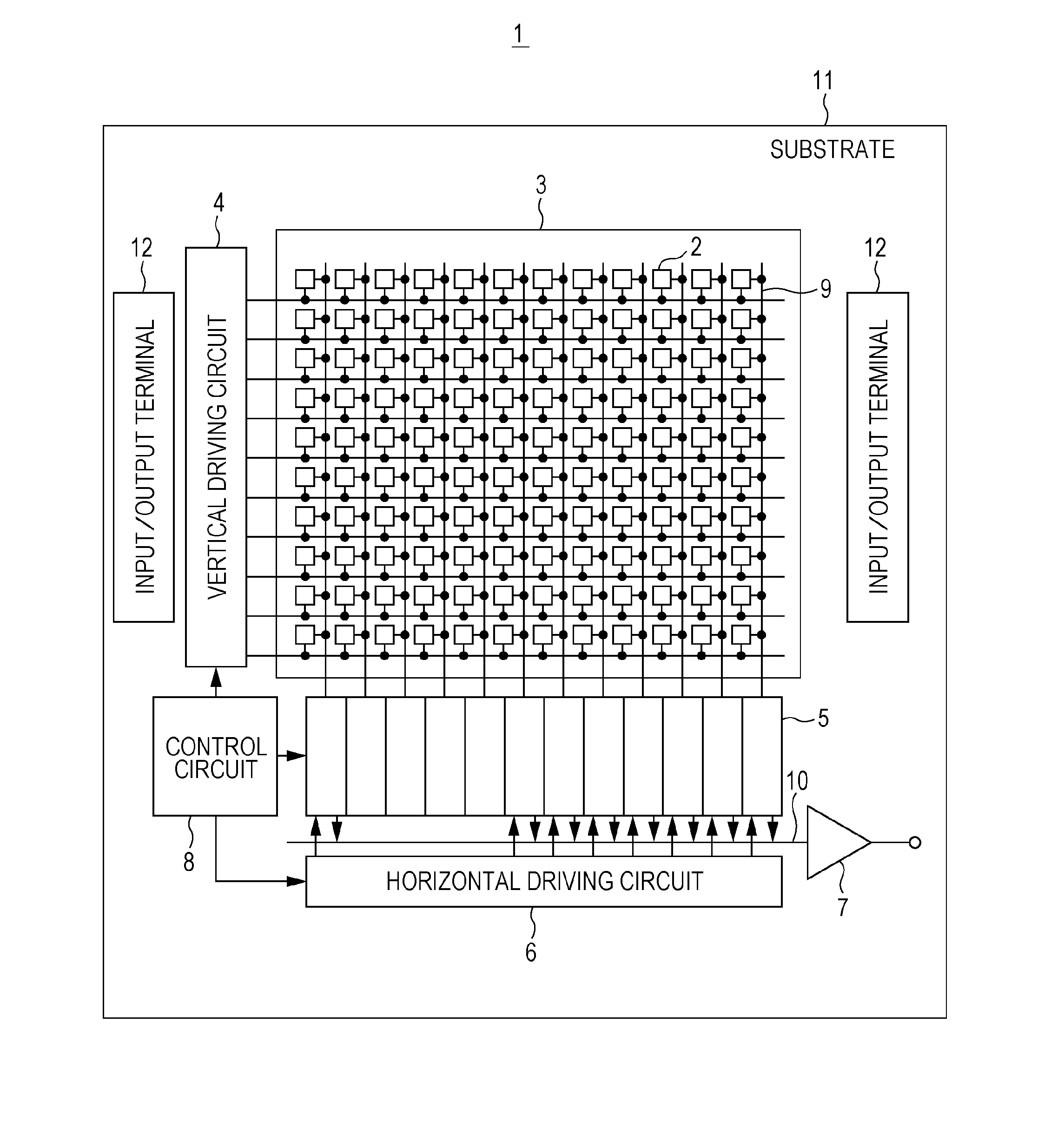
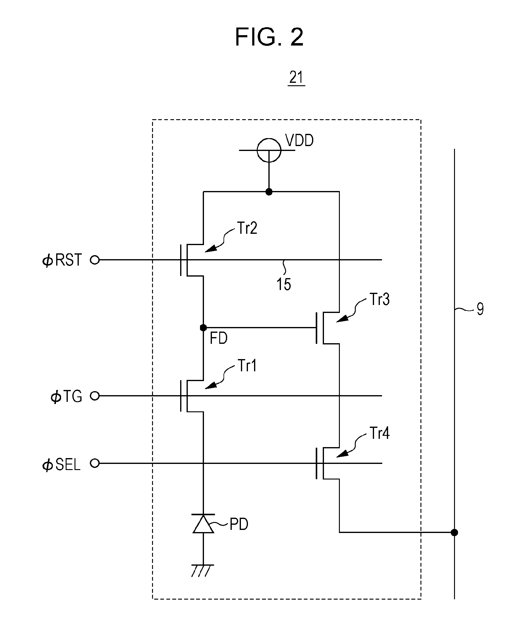
A solid-state imaging device includes multiple pixels formed of photoelectric converters and pixel transistors; a floating diffusion portion that exists within a region of each of the photoelectric converters when viewed from above; and a vertical transfer gate electrode of a transfer transistor that surrounds at least a portion of each photoelectric converter and is formed in the depth direction of a substrate and makes up the pixel transistor.
Description
BACKGROUND OF THE INVENTION[0001]1. Field of the Invention[0002]The present invention relates to a solid-state imaging device and manufacturing method thereof, a driving method of a solid-state imaging device, and electronic equipment applied to a camera or the like that has the solid-state imaging device therein.[0003]2. Description of the Related Art[0004]A CMOS solid-state imaging device has been used as a solid-state imaging device. A CMOS solid-state imaging device has low power source voltage and low power consumption, and therefore is used in digital still cameras, digital video cameras, and further various types portable terminal devices such as cellular telephones with built-in cameras.[0005]A CMOS solid-state imaging device is made up of a pixel region wherein multiple pixels that include photodiodes which are photoelectric converters and multiple pixel transistors are arrayed systematically and two-dimensionally, and a peripheral circuit portion that is disposed in the pe...
Claims
Login to View More Application Information
Patent Timeline
 Patent Type & AuthorityApplications(United States)
IPC IPC(8): H04N5/228H04N5/335H01L31/18H04N23/40H04N25/00
CPCH01L27/1461H01L27/14614H01L27/1463H01L27/14689H01L27/14641H01L27/14647H01L27/1464H01L27/14638
InventorYAMADA, AKIHIRO
OwnerSONY CORP