

Amplifier circuit and optical pickup device
- Summary
- Abstract
- Description
- Claims
- Application Information
AI Technical Summary
Benefits of technology
Problems solved by technology
Method used
Image

Examples
first embodiment
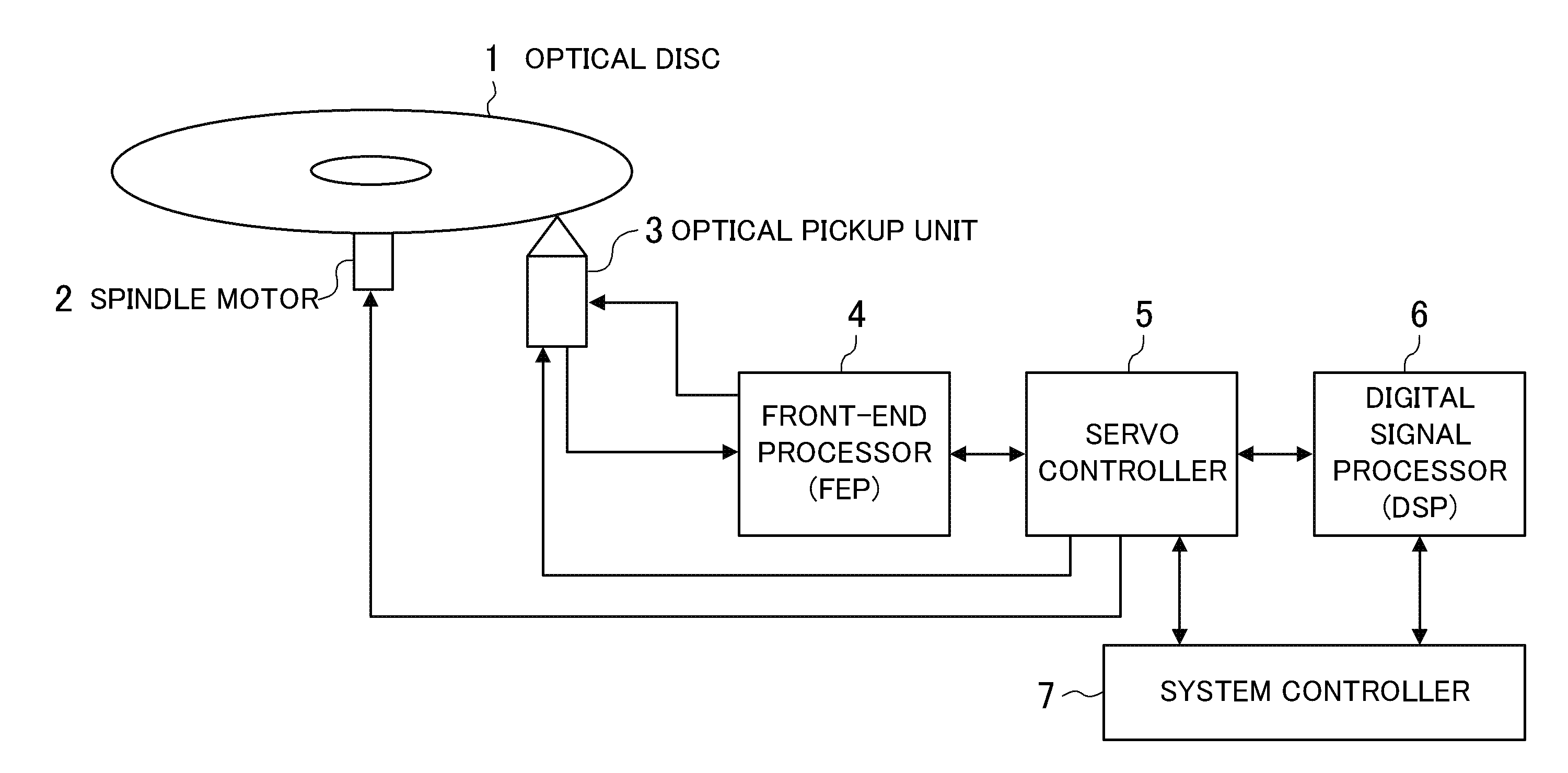
[0054]FIG. 1 illustrates an example of the whole configuration of an optical-disc drive which employs an amplifier circuit according to the present invention. In this case, general front end operations for BD (Blu ray Disc), DVD (Digital Versatile Disc), and CD (Compact Disc) are available.
[0055]Referring to FIG. 1, 1 denotes an optical disc (BD, DVD, or CD) put in the optical-disc drive, 2 denotes a spindle motor, 3 denotes an optical pickup unit, 4 denotes a front-end processor (FEP), 5 denotes a servo controller, 6 denotes digital signal processor (DSP), and 7 denotes a system controller. The optical pickup unit 3 applies a laser beam onto the optical disc 1 to detect the light reflected therefrom. The FEP 4 performs processing on the output of the optical pickup unit 3, such as analog operation and filtering. The FEP 4 also sends a predetermined signal to the optical pickup unit 3 depending on the optical disc type and the media type. The servo controller 5 controls the spindle ...
second embodiment
[0069]Referring next to FIG. 5, a second embodiment of the present invention is described.
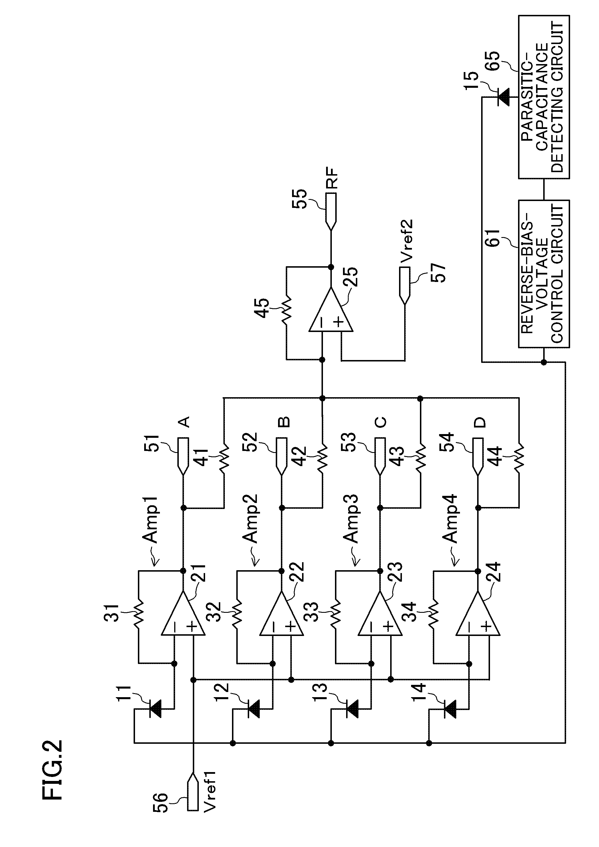
[0070]If the amount of the laser light incident on the photodiodes 11 to 14 of FIG. 2 is smaller, for reasons such that the optical pickup unit 3 of FIG. 1 makes a record on or plays an optical disc 1 having a low reflectivity, and that the optical system in the optical pickup unit 3 has a low transmission efficiency, the amplitudes of the signals outputted from the output terminals 51 to 54 and the RF output terminal 55 also become smaller. In this case, the signal-to-noise ratio when the front-end processor 4 performs signal processing in the later stage, thereby causing jitter and poor servo characteristics. Therefore, in this embodiment, an avalanche photodiode (APD) is employed for first photodiodes 11 to 14. This configuration prevents the signal-to-noise ratio from becoming worse even when the amount of incident laser light is smaller, thereby maintaining signal quality. This configurati...
third embodiment
[0082]Referring next to FIG. 8, a third embodiment of the present invention is described. In the first embodiment and the second embodiment, the photodiodes 11 to 14 of FIG. 2 successfully have stable optical sensitivities resistant to temperature change. In this embodiment, a description is given for the circuit configuration in which more stable control is achieved regardless of temperature change. The signal amplitudes of the output terminals 51 to 54 of FIG. 2 are determined by the electric currents generated in the photodiodes 11 to 14, and the feedback resistors 31 to 34. In order to achieve more stable control, the amount of variation in the resistance values of the feedback resistors 31 to 34 and the temperature changes thereof have to be reduced. Therefore, in this embodiment, a filter including a resistor and a parasitic capacitance is employed as the parasitic-capacitance detecting circuit 65 of FIG. 2. This configuration reduces the amount of variation in the optical sen...
PUM
 Abstract
Description
Claims
Application Information