

Semiconductor device and method of driving semiconductor device
- Summary
- Abstract
- Description
- Claims
- Application Information
AI Technical Summary
Benefits of technology
Problems solved by technology
Method used
Image

Examples
embodiment 1
[0065]In this embodiment, a circuit structure and operation of a semiconductor device which is one embodiment of the disclosed invention will be described with reference to FIG. 1, FIG. 2, FIG. 3, FIGS. 4A and 4B, and FIG. 5. In this embodiment, the case where n-channel transistors are used will be described.
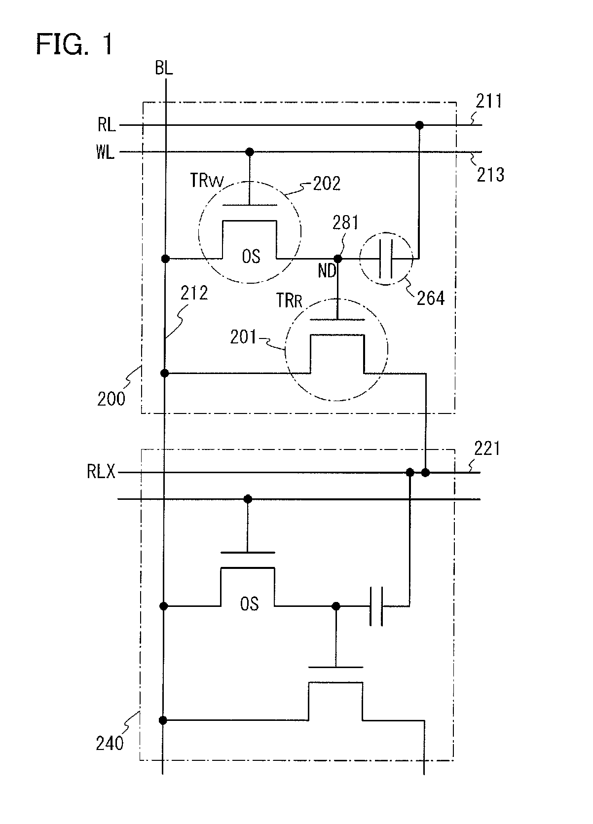
[0066]In FIG. 1, the circuit structure of the semiconductor device disclosed in this embodiment is illustrated. The semiconductor device illustrated in FIG. 1 includes a nonvolatile memory cell 200 including a first transistor 201, a second transistor 202, and a capacitor 264. In FIG. 1, a third wiring 213 (also referred to as a word line WL) and a gate electrode of the second transistor 202 (also referred to as a transistor TRW) are electrically connected to each other. One of a source electrode and a drain electrode of the second transistor 202, a gate electrode of the first transistor 201 (also referred to as a transistor TRR), and one electrode of the capacitor 264 are elect...
embodiment 2
[0135]In this embodiment, a semiconductor device having a structure different from that in Embodiment 1 is described with reference to FIG. 6, FIG. 7, and FIGS. 8A and 8B.
[0136]In FIG. 6, a circuit structure of the semiconductor device disclosed in this embodiment is illustrated. The semiconductor device illustrated in FIG. 6 includes a nonvolatile memory cell 250 including a first transistor 201, a second transistor 202, and a capacitor 264. In FIG. 6, a first wiring 211 (also referred to as a reading signal line RL) and one of a source electrode and a drain electrode of the first transistor 201 are electrically connected to each other. One of a source electrode and a drain electrode of the second transistor 202 (also referred to as a transistor TRW) and a gate electrode of the first transistor 201 (also referred to as a transistor TRR) are electrically connected to one electrode of the capacitor 264. A second wiring 212 (also referred to as a bit line BL) is electrically connected...
embodiment 3
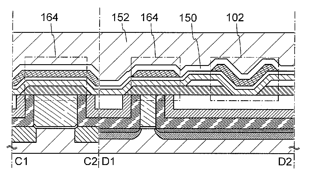
[0183]In this embodiment, a structure and a manufacturing method of a semiconductor device which is another embodiment of the disclosed invention will be described with reference to FIGS. 9A and 9B, FIGS. 10A to 10H, and FIGS. 11A to 11E.
[0184]In FIGS. 9A and 9B, an example of the structure of the semiconductor device is illustrated. FIG. 9A is a cross section of the semiconductor device, and FIG. 9B is a top view of the semiconductor device. Here, FIG. 9A corresponds to a cross section taken along lines A1-A2 and B1-B2 of FIG. 9B. The semiconductor device illustrated in FIGS. 9A and 9B includes a transistor 101 including a semiconductor material other than an oxide semiconductor, and a transistor 102 including an oxide semiconductor. The transistor including the semiconductor material other than the oxide semiconductor can be easily operated at high speed. On the other hand, the transistor including the oxide semiconductor can hold charge for a long time owing to its characteristic...
PUM
 Abstract
Description
Claims
Application Information