Microwell array chip and method of manufacturing same

a microwell array and array technology, applied in the field of microwell array chips, can solve the problems of cell sorter, expensive and complex method, and inability to identify individual antigen-specific lymphocytes within the group of lymphocytes

Active Publication Date: 2011-08-11
BLINK BIOMEDICAL SAS
View PDF26 Cites 115 Cited by
  • Summary
  • Abstract
  • Description
  • Claims
  • Application Information

AI Technical Summary

Problems solved by technology

However, it does not permit the identification of individual antigen-specific lymphocytes present within the group of lymphocytes.
However, the above detection method requires an expensive and complex device known as a cell sorter for separation.
(1) It is difficult to set the conditions in the device for separation; great skill is required to operate the device and separate cells;
(2) Due to high background noise, when the frequency of the antigen-specific lymphocyte is 0.1 percent or less, the antigen-specific lymphocyte cannot be detected;
(3) Cell separation efficiency is low;
(4) Time is required to separate low frequency cells; and
(5) Although the binding of antigen can be confirmed, the reaction by which the lymphocyte binds the antigen cannot be analyzed.
However, how the lymphocytes that have bound the antigen have reacted with the antigen (intracellular signal transmission, RNA synthesis, protein synthesis, or some other metabolic physiological reaction of the cell) cannot be analyzed.
Further, antigen-specific lymphocytes with a frequency of 0.1 or less cannot be detected.
However, no microwell array chip was known that could separately detect the antigen specificity of individual lymphocytes and permit recovery of the antigen-specific lymphocytes that were detected.
That is, in array chips in which multiple microwells are simply arrayed, there is a problem in that it is difficult to readily determine the position of a specific microwell.
In the above process, the present inventors further determined that when the array chip was washed after collecting the lymphocytes in the microwells using a cell suspension in the course of storing lymphocytes in microwells, there was a problem in that a large number of cells ended up flowing out of the microwells, causing the collection efficiency and filling rate to decrease markedly.

Method used


Image

  • Microwell array chip and method of manufacturing same
  • Microwell array chip and method of manufacturing same
  • Microwell array chip and method of manufacturing same

Examples


embodiments

Embodiment 1

(Fluorescent Marker)

[0250]FIG. 1 is an example of a Aspect of implementing the device of Aspect I of the present invention.

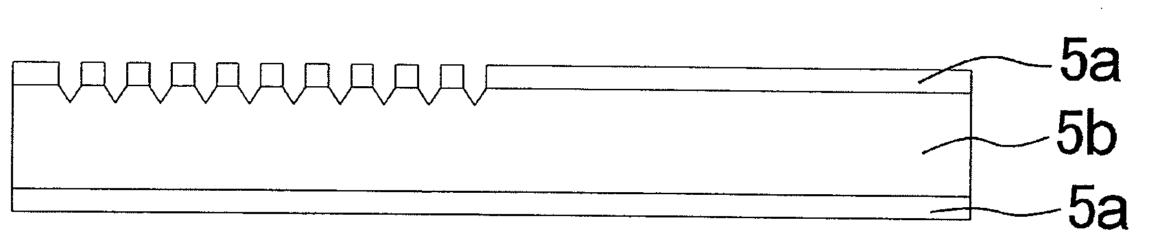
[0251]FIG. 1 shows a microwell array chip in which multiple microwells 1b have been formed on a substrate surface 1a of silicon material. Microwells 1b form clusters 1c of suitable numbers of units (for example, 10×10=100) to facilitate position identification. One use of the present microwell array chip is the introduction of a cell to which a fluorescent substance has been added into each well for evaluation, and the determination of fluorescent emission. In this process, those cells not emitting fluorescence cannot be observed because observation by fluorescence microscope or fluorescence scanner is conducted with specifications based on the wavelength of fluorescence. Accordingly, as shown in FIG. 1, a minute marker 1d of a fluorescent substance is formed between the individual clusters.

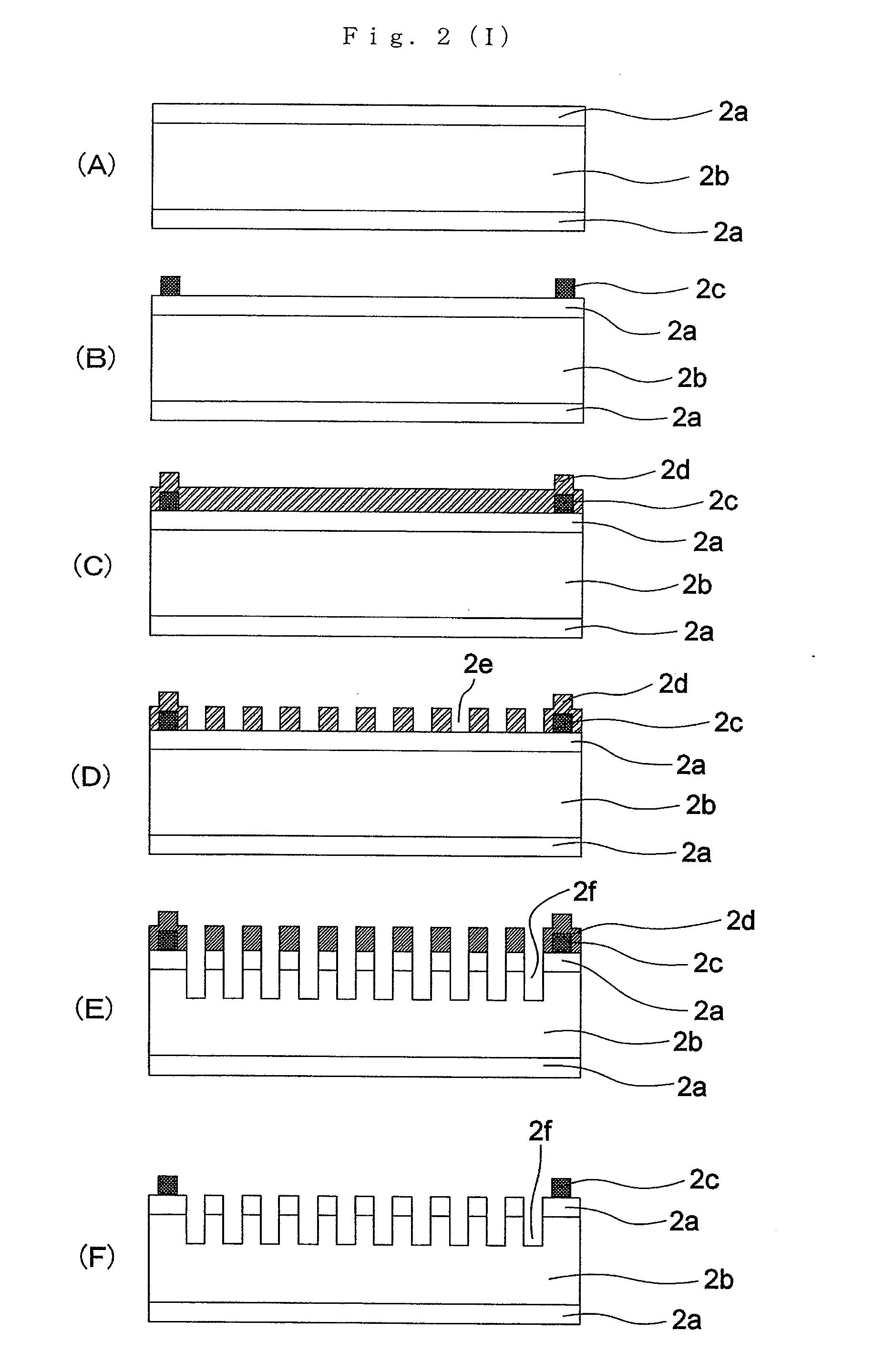
[0252]The method of manufacturing these markers is given bel...

embodiment 2

(Reflective Marker)

[0268]FIG. 3 is an implementation Aspect of a reflective marker 3d that is observable by observing scattered light with a fluorescence microscope or fluorescence scanner by forming dips and rises on silicon substrate 3a. It is used as a marker for identifying the positions of clusters of multiple microwells 3b arrayed on silicon substrate 3a. By forming indentation 3e by etching or the like on the substrate and directing a fluorescence excitation beam to an observation device by means of irregular reflection, it is possible to identify the position of the indentation.

[0269]FIG. 4 shows the principle involved. For the surface of a substrate 4a without anything, such as the dips or rises shown on the left side of the figure, no excitation light enters the observation device due to full reflection. However, when the indentations on the right side scatter the excitation beam radially, reflected light enters the optical system of the observation device and can be ident...

embodiment 3

A Lip-Structure Embodiment

[0279]FIG. 7 shows a microwell structure fabricated based on Aspect II of the present invention.

[0280]The present structure can be achieved by selecting an upper thin film of a material that is easy to process with a semiconductor substrate, resin substrate, or the like. The microwells 13 that are formed on the surface of (100) surface silicon substrate 11 measure from several micrometers to several tens of micrometers in both opening diameter and depth. The surface on which no wells are formed is covered with a thin film layer 12′ in the form of an oxide film, metal film, or the like. The substrate is etched to form well openings 13a, in which are found eave-shaped protrusions 14 of thin film layer 12′. The thickness of thin film layer 12′ is controlled to from several hundred nanometers to several micrometers during formation. Eave-shaped protrusions 14 formed of thin film layer 12′ are achieved by an etching method in which thin film layer 12′ is etched ...


PUM

PropertyMeasurementUnit
diameteraaaaaaaaaa
diameteraaaaaaaaaa
depthaaaaaaaaaa

Abstract

The present invention is directed to a microwell array chip made of silicon and having multiple microwells. Each microwell is used to store a single specimen organic cell. Each microwell is of a size and shape holding just one organic cell, and the interior surface of the microwells are coated with a fluorocarbon film.

Description

[0001]This application is a Continuation of and claims the benefit of co-pending U.S. application Ser. No. 10 / 573,289, filed Feb. 20, 2007, which is the national stage of PCT Application No. PCT / JP2004 / 014285 filed on Sep. 22, 2004. Benefit of priority is also claimed to JP 2003-333363 filed on Sep. 25, 2003, JP 2003-336771 filed on Sep. 29, 2003 and JP 2003-336793 filed Sep. 29, 2003. The entire contents of each of the above documents is hereby incorporated by reference.TECHNICAL FIELD[0002]Aspect I of the present invention relates to a microwell array chip that can be used to detect organic cells such as antigen-specific lymphocytes. In particular, Aspect I of the present invention relates to a microwell array chip in which the position of a given microwell is readily determined.[0003]Aspect II of the present invention relates to a microwell array chip, and a method for manufacturing the same, having good collection efficiency of organic cells in and recovery efficiency of organic...

Claims


Application Information

Patent Timeline
Patent Type & Authority Applications(United States)
IPC IPC(8): C12N5/078G01N33/53G01N33/543G01N37/00
CPCG01N33/54366B01J2219/00659A61K48/00A61K35/12B01J19/0046C12M23/12G01N33/53G01N37/00
Inventor MURAGUCHI, ATSUSHIKISHI, HIROYUKITOKIMITSU, YOSHIHARUKONDO, SACHIKOOBATA, TSUTOMUFUJIKI, SATOSHIYOKOYAMA, YOSHIYUKINABESAWA, HIROFUMITAKABAYASHI, SOTOHIROTANINO, KATSUMI
Owner BLINK BIOMEDICAL SAS
Why Eureka
Try Eureka