

Photovoltaic devices using semiconducting nanotube layers
- Summary
- Abstract
- Description
- Claims
- Application Information
AI Technical Summary
Benefits of technology
Problems solved by technology
Method used
Image

Examples
Embodiment Construction
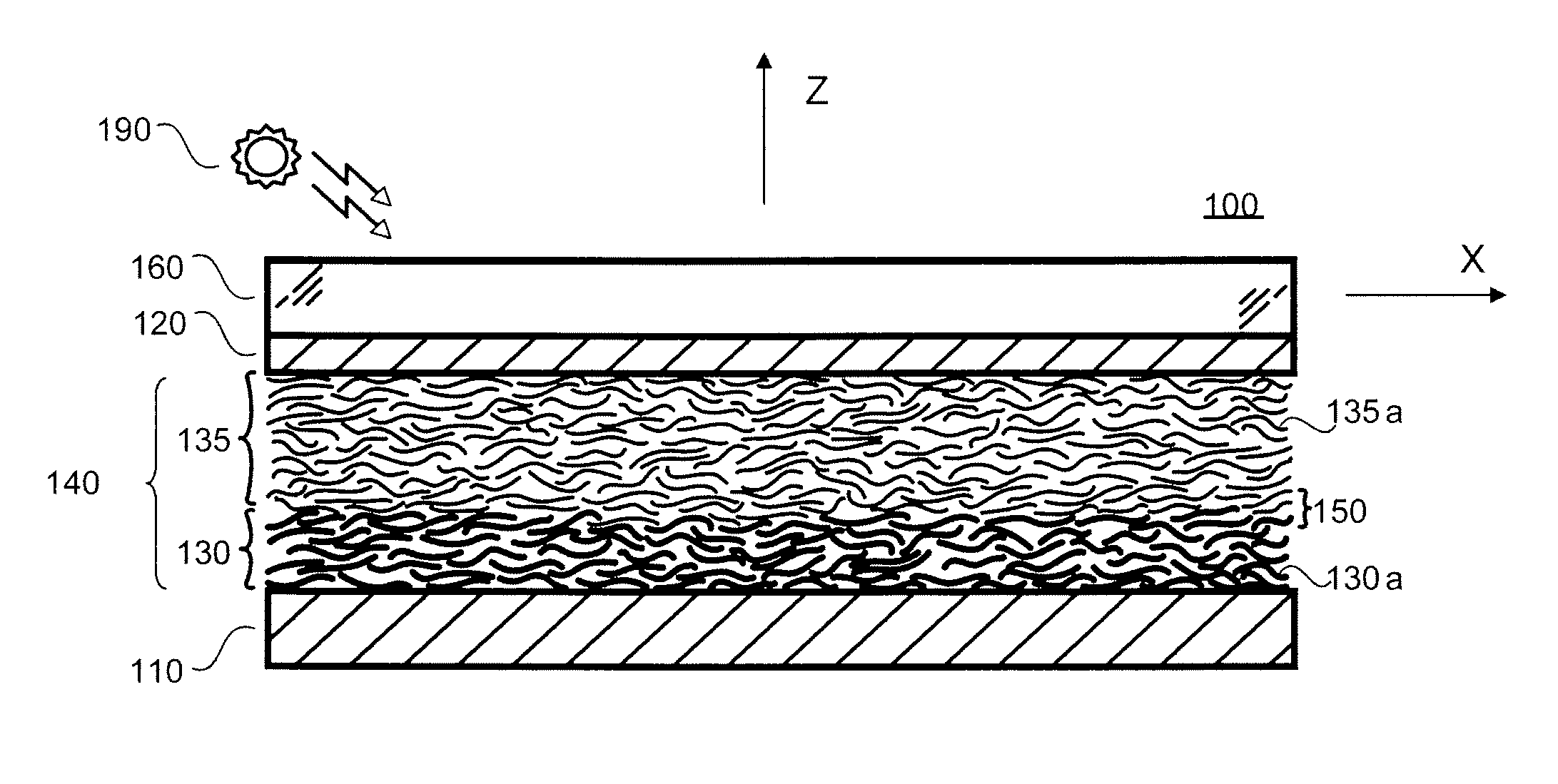
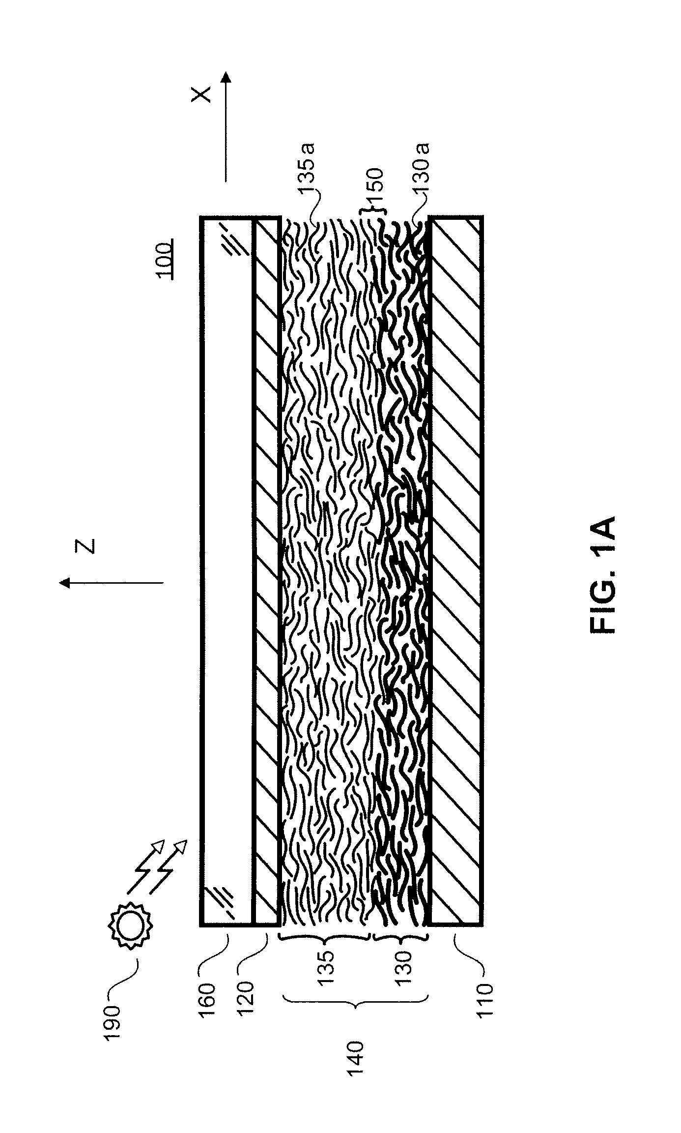
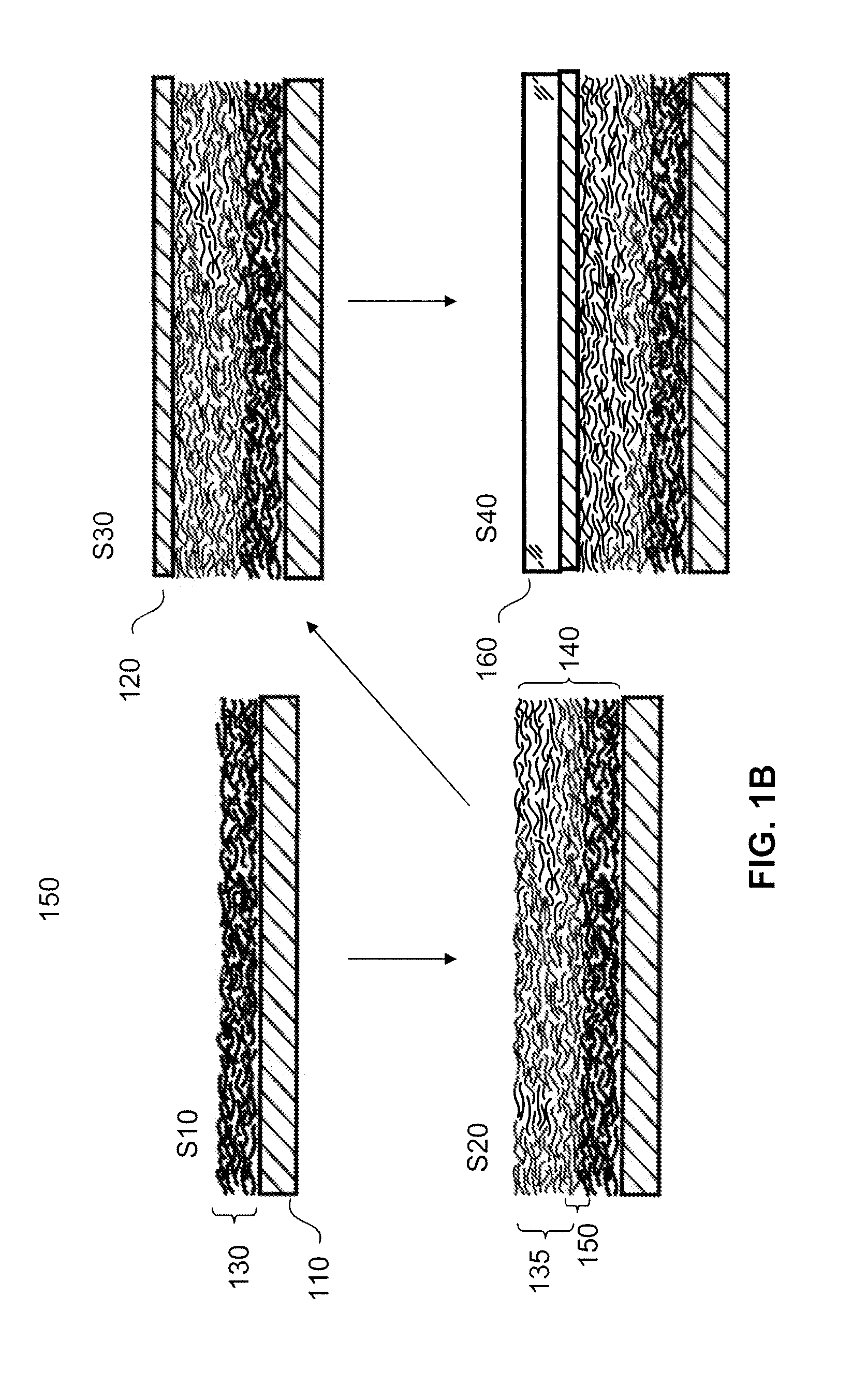
[0046]The present disclosure teaches a plurality of photovoltaic (PV) devices which use layers of semiconducting carbon nanotubes as the light absorption layer.
[0047]In some embodiments of the present disclosure a p-n junction PV device is realized by forming a layer of p-type semiconducting carbon nanotubes adjacent to a layer of n-type semiconducting carbon nanotubes, creating a p-n junction across the interface of the two layers. Within such embodiments, the p-type carbon nanotube layer acts as a light absorption material, releasing valance electrons into the conduction band of the nanotube structures when photons are absorbed. In some aspects of these embodiments, these p-type carbon nanotube layers include photosensitive particles such as, but not limited to, photosensitive dyes such as ruthenium-polypyridine and quantum dots made from III-V compounds such as GaAs, GaSb, and InP or II-VI compounds such as CdS, CdSe, ZnS, and ZnSe. Such nanoparticles can be dispersed in the nano...
PUM
 Abstract
Description
Claims
Application Information