Photosensor device

a technology of photosensors and sensors, applied in the field of photosensor devices, can solve the problems of poor sensitivity, high cost, and extremely high cost, and achieve the effect of low voltage and simple structur

Active Publication Date: 2011-09-08
PANASONIC LIQUID CRYSTAL DISPLAY CO LTD +1
View PDF3 Cites 2 Cited by
  • Summary
  • Abstract
  • Description
  • Claims
  • Application Information

AI Technical Summary

Benefits of technology

[0021]According to the present invention, it is possible to provide a photosensor device that is simple in structure and can be driven with low voltage by using photodiodes produced using amorphous silicon or microcrystal silicon.

Problems solved by technology

However, production of relatively-large area sensors results in a problem of high cost.
Use of the photo area sensors in personal computers and cell phones as area sensors for biometric authentication leads to extremely-high cost.
Some sensors are put to practical use in some applications and others are not because they are poor in sensitivity.
It is difficult to produce a high-performance sensor on a glass substrate because only amorphous silicon or microcrystal silicon which is poorer in performance than single-crystal silicon is available on the glass substrate.
However, if sensors are produced without single-crystal silicon, the performance of the transistor deteriorates and variations of amplifiers cannot be appropriately corrected, resulting in fixed noise.

Method used


Image

  • Photosensor device
  • Photosensor device
  • Photosensor device

Examples


first embodiment

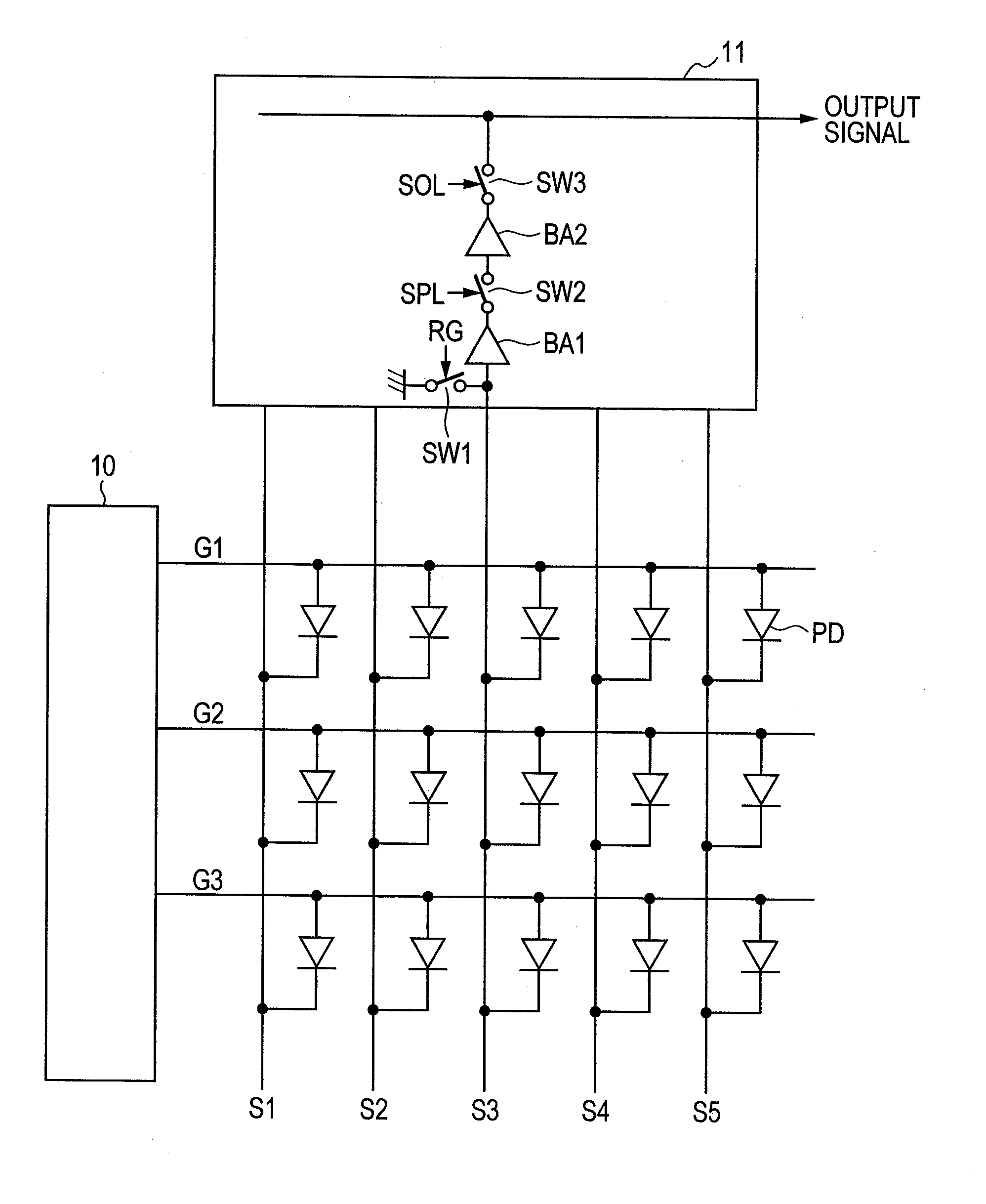
[0030]FIG. 1 is a circuit diagram for showing a circuit configuration of a photosensor device according to a first embodiment of the present invention.

[0031]As shown in FIG. 1, the photosensor device of the embodiment includes a diode matrix array in which plural photodiodes PD are arranged in a matrix shape and which configures a light receiving surface, plural scanning lines (G1, G2, G3, . . . ) which are coupled to anodes of the photodiodes PD in the respective lines of the photodiode array, plural read lines (S1, S2, S3, S4, S5, . . . ) which are coupled to cathodes of the photodiodes PD in the respective columns of the photodiode array, a vertical gate driver 10 which is coupled to the respective scanning lines (G1, G2, G3, . . . ) and sequentially selects the scanning lines (G1, G2, G3, . . . ) in each horizontal scanning period, and a signal processing circuit 11 which is coupled to the respective read lines (S1, S2, S3, S4, S5, . . . ) and loads each voltage fluctuation of t...

second embodiment

[0046]FIG. 4 is a circuit diagram for showing a circuit configuration of a photosensor device according to a second embodiment of the present invention.

[0047]In the embodiment, the polarities of the photodiodes PD in the first embodiment are inversed. In this case, the polarities of the driving voltage and the signal voltage are also inversed.

[0048]Specifically, when the signal RG becomes the H-level and the switch circuit SW1 in the signal processing circuit 11 are turned on in a blanking period of one horizontal scanning period HSYNC, each of the read lines (S1, S2, S3, S4, S5, . . . ) is adjusted to, for example, electric potential at the H-level in a driving method of the photosensor device of the embodiment.

[0049]Further, during a period when the signal RG is at the H-level, each voltage level of the scanning lines (G1, G2, G3, . . . ) becomes the H-level. When the signal RG becomes the L-level, each voltage level of the scanning lines (G1, G2, G3, . . . ) becomes the L-level.

[...

third embodiment

[0053]FIG. 5 is a timing view for explaining a driving method of a photosensor device according to a third embodiment of the present invention.

[0054]In the embodiment, the sensitivity varies by changing the selection period (the H-level period in FIG. 3) of each of the scanning lines (G1, G2, G3, . . . ) in the first embodiment.

[0055]It should be noted that only the scanning line G1 is illustrated in FIG. 5. However, the same is true for the other scanning lines. Further, the signal RG used to reset each voltage of the read lines (S1, S2, S3, S4, S5, . . . ) and the signal SPL used to load a signal are the same as those in the first embodiment.

[0056]In a period 1 of FIG. 5, the H-level period of the scanning line G1 corresponds to one horizontal scanning period HSYNC, and the rising time of each electric potential of the read lines (S1, S2, S3, S4, S5, . . . ) is longest. Therefore, the signal voltage loaded to the signal processing circuit 11 becomes highest, resulting in the best ...


PUM


Abstract

The present invention provides a photosensor device including: a photodiode array in which photodiodes are arranged in an array shape; scanning lines which are coupled to first electrodes of the photodiodes in respective lines of the photodiode array; read lines which are coupled to second electrodes of the photodiodes in respective columns of the photodiode array; a scanning circuit which is coupled to the scanning lines and sequentially supplies a selected scanning signal to the respective scanning lines in each horizontal scanning period; and a signal processing circuit which is coupled to the read lines and loads each voltage fluctuation of the read lines in one horizontal scanning period as signal voltage when reading a signal, wherein each of the photodiodes is made of amorphous silicon or microcrystal silicon, and forward bias voltage is applied to each of the photodiodes when reading a signal.

Description

CLAIM OF PRIORITY[0001]The present application claims priority from Japanese Patent Application JP 2010-050026 filed on Mar. 8, 2010, the content of which is hereby incorporated by reference into this application.BACKGROUND OF THE INVENTION[0002]1. Field of the Invention[0003]The present invention relates to a photosensor device such as a photo area sensor, and particularly to a photosensor device using photodiodes which are produced using amorphous silicon or microcrystal silicon.[0004]2. Description of the Related Art[0005]Photo area sensors are currently used in not only digital cameras, but also cell phone cameras, cell phone video cameras, fingerprint authentication apparatuses, and finger authentication apparatuses.[0006]As these photo area sensors, CCDs and CMOS sensors are currently used. CCDs and CMOS sensors are produced using single-crystal silicon, and are excellent in sensitivity and resolution.[0007]However, production of relatively-large area sensors results in a prob...

Claims


Application Information

Patent Timeline
Patent Type & Authority Applications(United States)
IPC IPC(8): H04N5/228
CPCY02E10/50H04N5/228H04N25/76H04N23/40
Inventor YASUDA, KOZOMIYAZAWA, TOSHIO
Owner PANASONIC LIQUID CRYSTAL DISPLAY CO LTD
Why Eureka
Try Eureka