Semiconductor device

Inactive Publication Date: 2011-09-22
SEMICON ENERGY LAB CO LTD
View PDF99 Cites 36 Cited by
  • Summary
  • Abstract
  • Description
  • Claims
  • Application Information

AI Technical Summary

Benefits of technology

[0026]Further, in one embodiment of the present invention, a gate electrode of a transistor including an oxide semiconductor material and a capacitor electrode are formed using different conductive layers, and an insulating layer which covers the transistor is formed o

Problems solved by technology

A transistor formed using a purified oxide semiconductor can hold dat

Method used


Image

  • Semiconductor device
  • Semiconductor device
  • Semiconductor device

Examples


embodiment 1

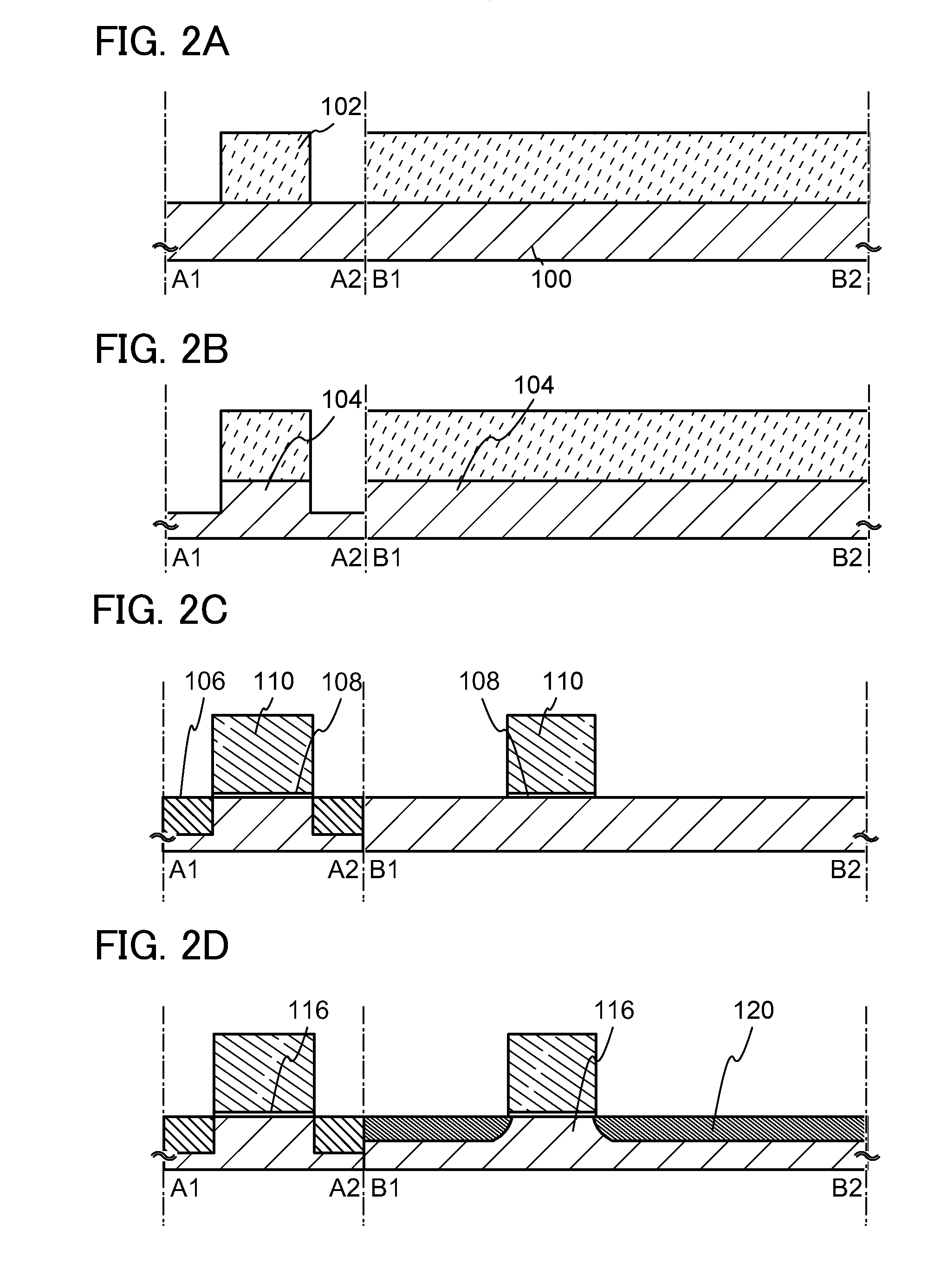
[0048]In this embodiment, a structure and a manufacturing method of a semiconductor device according to one embodiment of the present invention will be described with reference to FIGS. 1A and 1B, FIGS. 2A to 2D, FIGS. 3A to 3D, FIGS. 4A to 4D, FIGS. 5A to 5C, and FIGS. 6A and 6B.

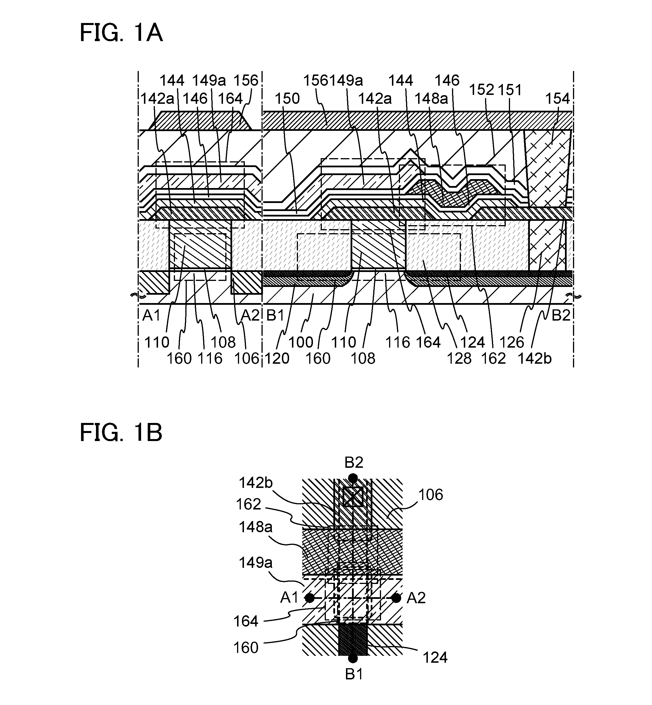
[0049]FIGS. 1A and 1B illustrate an example of a structure of a semiconductor device. FIG. 1A is a cross-sectional view of the semiconductor device, and FIG. 1B is a plan view of the semiconductor device. Here, FIG. 1A illustrates a cross section taken along line A1-A2 and line B1-B2 in FIG. 1B. The semiconductor device illustrated in FIGS. 1A and 1B includes a transistor 160 including a first semiconductor material in a lower portion, and a transistor 162 including a second semiconductor material in an upper portion. Here, it is preferable that the first semiconductor material and the second semiconductor material be different from each other. For example, the first semiconductor material can be a semicond...

embodiment 2

[0155]In this embodiment, a structure and a manufacturing method of a semiconductor device according to another embodiment of the disclosed invention will be described with reference to FIGS. 7A and 7B, FIGS. 8A to 8H, FIGS. 9A to 9E, and FIGS. 10A and 10B.

[0156]FIGS. 7A and 7B illustrate an example of a structure of the semiconductor device according to this embodiment. FIG. 7A is a cross-sectional view of the semiconductor device, and FIG. 7B is a plan view of the semiconductor device. Here, FIG. 7A illustrates a cross section taken along line E1-E2 and line F1-F2 in FIG. 7B. The semiconductor device illustrated in FIGS. 7A and 7B includes a transistor 560 including a first semiconductor material in the lower portion, and a transistor 562 including a second semiconductor material in the upper portion. Here, it is preferable that the first semiconductor material and the second semiconductor material be different from each other. For example, the first semiconductor material can be ...

modification example

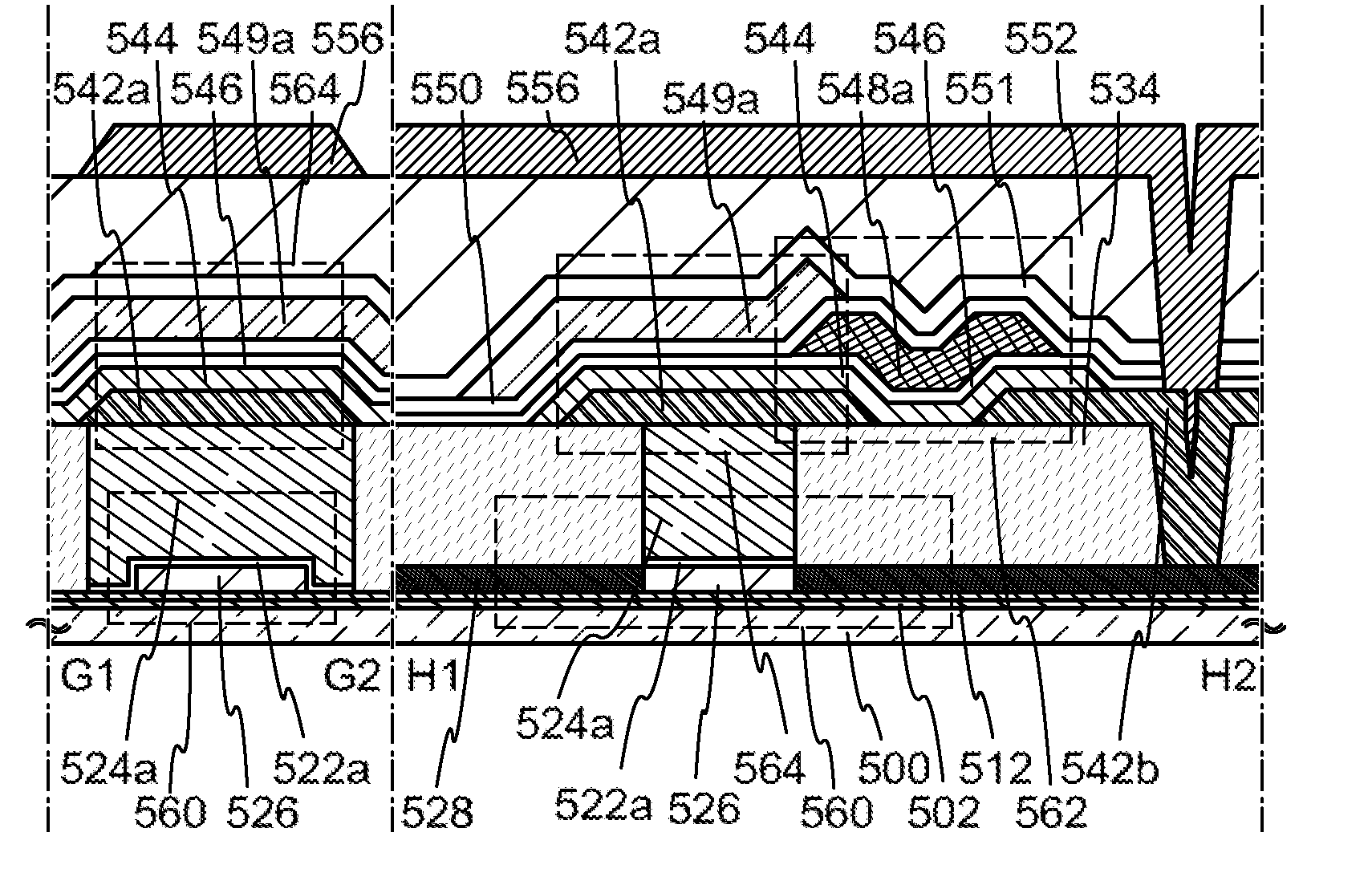
[0211]Next, another structure of the semiconductor device in FIGS. 7A and 7B will be described with reference to FIGS. 10A and 10B.

[0212]FIG. 10A is a cross-sectional view of the semiconductor device, and FIG. 10B is a plan view of the semiconductor device. Here, FIG. 10A illustrates a cross section taken along line G1-G2 and line H1-H2 in FIG. 10B. The semiconductor device illustrated in FIGS. 10A and 10B, like the semiconductor device illustrated in FIGS. 7A and 7B, includes the transistor 560 including a first semiconductor material in the lower portion, and the transistor 562 including a second semiconductor material in the upper portion. Here, it is preferable that the first semiconductor material and the second semiconductor material be different from each other. For example, the first semiconductor material can be a material (silicon) which is not an oxide semiconductor and the second semiconductor material can be an oxide semiconductor. A transistor including a semiconductor...


PUM


Abstract

A semiconductor device with a novel structure is provided in which stored data can be held even when power is not supplied and the number of writing is not limited. The semiconductor includes a second transistor and a capacitor over a first transistor. The capacitor includes a source or drain electrode and a gate insulating layer of the second transistor and a capacitor electrode over an insulating layer which covers the second transistor. The gate electrode of the second transistor and the capacitor electrode overlap at least partly with each other with the insulating layer interposed therebetween. By forming the gate electrode of the second transistor and the capacitor electrode using different layers, an integration degree of the semiconductor device can be improved.

Description

TECHNICAL FIELD[0001]The disclosed invention relates to a semiconductor device including a semiconductor element and a manufacturing method thereof.BACKGROUND ART[0002]Memory devices including semiconductor elements are broadly classified into two categories: a volatile memory device that loses stored data when not powered, and a nonvolatile memory device that holds stored data even when not powered.[0003]A typical example of a volatile memory device is a dynamic random access memory (DRAM). A DRAM stores data in such a manner that a transistor included in a memory element is selected and charge is accumulated in a capacitor.[0004]When data is read from a DRAM, charge in a capacitor is lost owing to the above principle; thus, writing is necessary every time data is read out. Moreover, since leakage current (off-state current) flows between a source and a drain of a transistor included in a memory element when the transistor is in an off state, charge flows into or out even when the ...

Claims


Application Information

Patent Timeline
IPC IPC(8): H01L27/088
CPCG11C16/0408H01L27/0688H01L27/115H01L28/60H01L27/11551H01L27/1156H01L27/1225H01L27/11521H10B41/70H10B41/20H10B69/00H10B41/30H01L21/31051H10B10/125
Inventor KATO, KIYOSHINAGATSUKA, SHUHEI
Owner SEMICON ENERGY LAB CO LTD
Why Eureka
Try Eureka