Organic electric field light-emitting element

a technology of electric field and light-emitting element, which is applied in the direction of discharge tube luminescnet screen, other domestic articles, organic semiconductor devices, etc., can solve the problems of chromaticity change, chromaticity change, and no consideration is paid for preventing chromaticity change, so as to improve emission efficiency and permanence, the effect of preventing a chromaticity change of emission

Active Publication Date: 2011-09-22
UDC IRELAND
View PDF3 Cites 4 Cited by
  • Summary
  • Abstract
  • Description
  • Claims
  • Application Information

AI Technical Summary

Benefits of technology

[0024]The present invention can solves the problems in the art, and provides an organic electric field light-emitting element having improved emission efficiency and permanence, as well as preventing a chromaticity change of emission at the time when current density is changed.

Problems solved by technology

Such organic electric field light-emitting element loses its carrier balance when the current density changes, which causes decreased emission efficiency or permanence, and chromaticity changes of emission.
Among these problems, the main factor for causing the chromaticity change is an influence from optical interference due to the change of the location where light is emitted.
However, the control of the luminescent material concentration disclosed in the patent literatures is aimed to improve emission efficiency and permanence by controlling a carrier balance, and no consideration is paid for preventing chromaticity change caused by current density.

Method used


Image

  • Organic electric field light-emitting element
  • Organic electric field light-emitting element
  • Organic electric field light-emitting element

Examples


example 1

Preparation of White Association Emission Light-Emitting Element

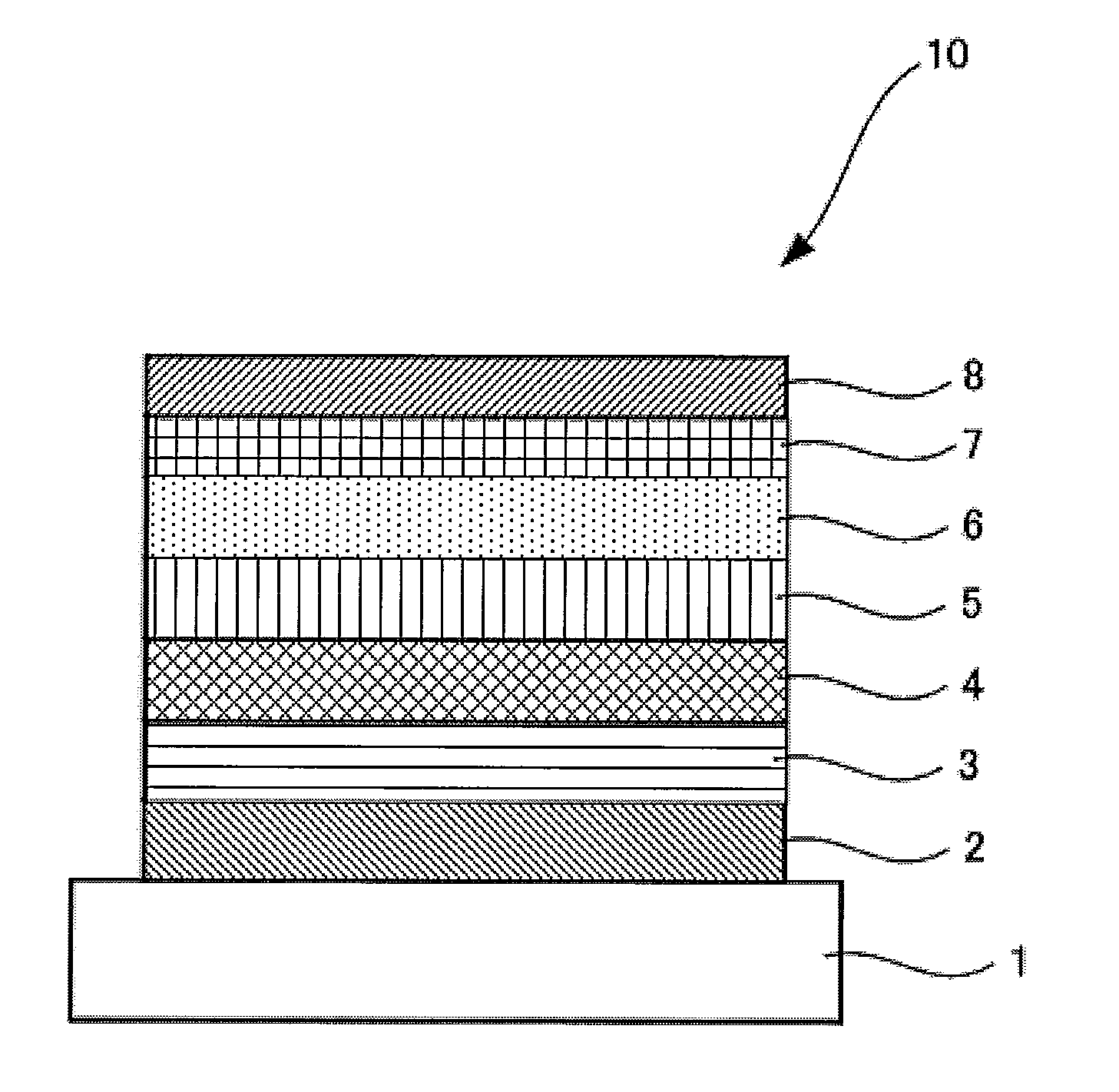
[0167]A glass substrate having a thickness of 0.5 mm and a side of 2.5 cm was placed in a washing container, and subjected to ultrasonic washing in a neutral detergent, and then subjected to ultrasonic washing in purified water. Thereafter, the glass substrate was subjected to heat treatment at 120° C. for 120 minutes, followed by subjected to UV-ozone treatment for 30 minutes. On this glass substrate, each layer was deposited by vacuum deposition. Note that, in the following Examples and Comparative Examples, the deposition speed was 0.2 nm / sec unless otherwise stated. The deposition speed was measured by a quartz resonator. Moreover, the thickness of each layer was measured by a quartz resonator.

[0168]At first, on the glass substrate, indium tin oxide (ITO) was deposited by sputtering to give a thickness of 100 nm to thereby form an anode.

[0169]Next, on the anode (ITO), 4,4′,4″-tris(N,N-(2-naphthyl)-phenylamino)triphe...

example 2

Preparation of White Emission Single Layer Light-Emitting Element

[0185]A organic electric field light-emitting element of Example 2 was prepared in the same manner as in Example 1, provided that mCP was doped with 15% by mass of Compound 3 expressed by the following structural formula, 0.13% by mass of Compound 4 expressed by the following structural formula, and Compound 5 where the doping amount of Compound 5 was continuously changed from 0.13% by mass (at the side of Compound 1) to 0.2% by mass (at the side of Balq), all relative to the amount of mCP.

[0186]The layer structure of the organic electric field light-emitting element of Example 2 was as presented below. Note that, the values given in the brackets indicate the thickness of each layer.

example 3

Preparation of White Emission Single Layer Light-Emitting Element

[0191]An organic electric field light-emitting element of Example 3 was prepared in the same manner as in Example 1, provided that mCP was doped with Compound 3 expressed by the structural formula above where the doping amount thereof was continuously changed from 15% by mass (at the side of Compound 1) to 13% by mass (at the side of Balq), 0.13% by mass of Compound 4 expressed by the structural formula above, and 0.13% by mass of Compound 5 expressed by the structural formula above, all relative to the amount of mCP.

[0192]The layer structure of the organic electric field light-emitting element of Example 3 was as presented below. Note that, the values given in the brackets indicate the thickness of each layer.


PUM


Abstract

An organic electric field light-emitting element, which contains: an anode; a cathode; and a light-emitting layer provided between the anode and the cathode, wherein the light-emitting layer contains two or more luminescent materials each giving a different emission peak, and a concentration ratio [(B/A)×100] in the light-emitting layer gradually increases along with the direction from an anode side of the light-emitting layer to a cathode side of the light-emitting layer, where A denotes a concentration of the luminescent material having the emission peak at the shortest wavelength side compared to the emission peaks of other luminescent materials, and B denote a concentration of the luminescent material having the emission peak at the longest wavelength side compared to the emission peaks of other luminescent materials, and wherein the light-emitting layer satisfies the relationship of: [(B/A)×100]≦10%.

Description

BACKGROUND OF THE INVENTION[0001]1. Field of the Invention[0002]The present invention relates to an organic electric field light-emitting element (may also referred to as an “organic electroluminescence element”, an “organic EL element”, and the like).[0003]2. Description of the Related Art[0004]Organic electric field light-emitting elements have characteristics such as of self luminescence and high-speed response, and hence are expected as applications for flat panel displays. Especially since a two layer (laminate) type of organic electric field light-emitting elements, in which a thin hole-transporting organic film (i.e. a hole transporting layer) and a thin electron-transporting organic film (i.e. an electron transporting layer) are laminated were reported, organic electric field light-emitting elements attracted great deals of interests as large-scale luminescence elements which emits light with low voltage of 10 V or lower. The basic structure of the laminate type of the organ...

Claims


Application Information

Patent Timeline
Patent Type & Authority Applications(United States)
IPC IPC(8): H01J1/62
CPCC09K11/06Y10S428/917C09K2211/1029C09K2211/1044C09K2211/185H01L51/0072H01L51/0081H01L51/0085H01L51/0087H01L51/5012H01L51/5016H01L51/5036H01L51/5048H01L2251/5346H05B33/14C09K2211/1007H10K85/324H10K85/346H10K85/342H10K85/6572H10K50/125H10K50/14H10K50/11H10K2101/10H10K2101/80
Inventor YASUDA, HIDEKISATOH, TASUKU
Owner UDC IRELAND
Why Eureka
Try Eureka