Eureka AIR delivers breakthrough ideas for toughest innovation challenges, trusted by R&D personnel around the world.

Through Glass Via Manufacturing Process

Inactive Publication Date: 2011-09-22
QUALCOMM INC
View PDF6 Cites 30 Cited by
  • Summary
  • Abstract
  • Description
  • Claims
  • Application Information

AI Technical Summary

Problems solved by technology

Direct application of the Bosch process can not be implemented with glass, however, because no etch plasma has a high enough etch rate of glass, especially while etching within the same plasma chamber as with other etches of the process.
This Bosch process is inefficient for glass, however, because plasma etches glass at a very slow rate.
However, wet etching is usually an isotropic etching process, resulting in very large vias.
However, because the holes are manufactured one hole at a time, the time to drill many holes will generally be quite extensive, thus, decreasing manufacturing throughput.
Moreover, laser drilled holes are relatively large.

Method used


Image

  • Through Glass Via Manufacturing Process
  • Through Glass Via Manufacturing Process
  • Through Glass Via Manufacturing Process

Examples


Embodiment Construction

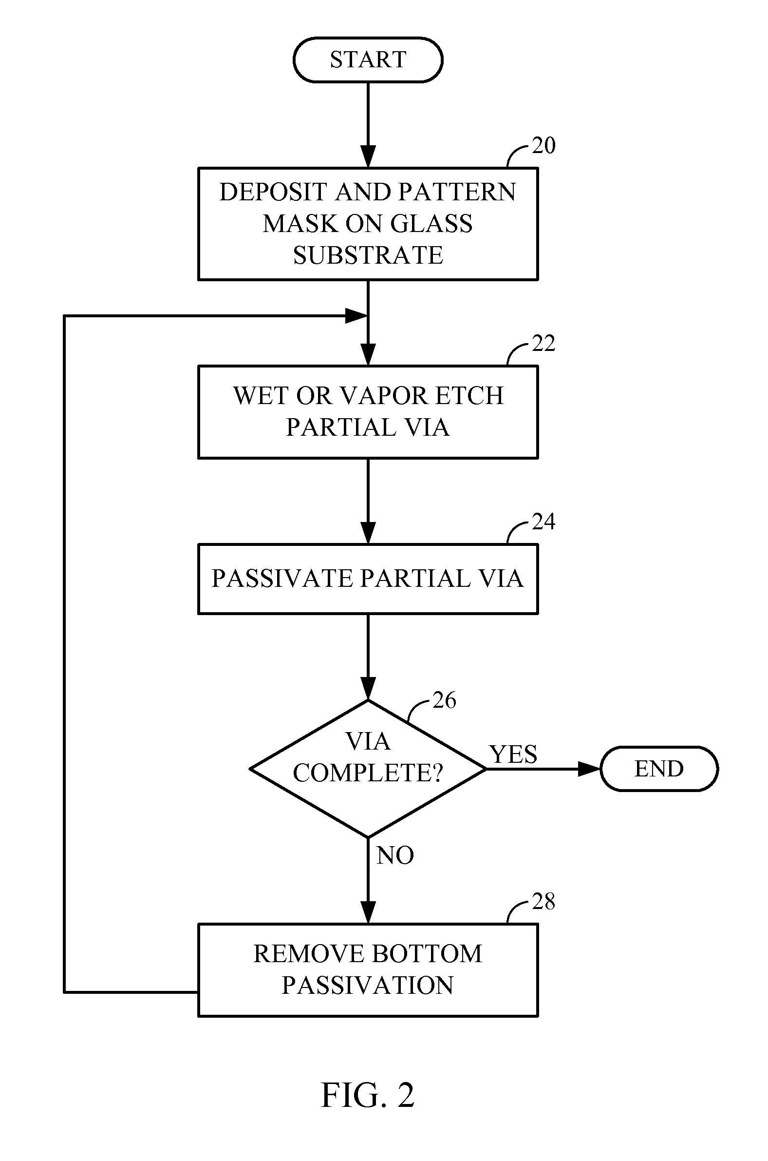
[0014]An improved process for manufacturing through glass vias within a glass substrate is explained. This low cost process has a relatively quick etch rate, and results in vias with a relatively small pitch and a relatively high aspect ration.

[0015]Referring now to FIGS. 2-6, an exemplary process for manufacturing a through glass via will be discussed.

[0016]At block 20, a photoresist mask 32 is deposited on a relatively thick glass substrate 30. In one embodiment the glass substrate 30 is approximately 200 microns thick. The photoresist mask 32 is patterned to create openings 34 where the vias will be fabricated. The patterned photoresist becomes a hard mask 32 for the upcoming non-plasma etch. Exemplary materials for the photoresist include silicon nitride (SiN), silicon carbide (SiC), and the like.

[0017]At block 22, a vapor of an oxide etch chemical, or a wet oxide etch chemical is applied in a chamber containing the substrate 30 to create a shallow partial via 40. In one embodim...


PUM

PropertyMeasurementUnit
Thicknessaaaaaaaaaa
Etch rateaaaaaaaaaa
Aspect ratioaaaaaaaaaa

Abstract

Fabrication of a through glass via in a relatively thick glass substrate includes patterning a through glass via hard mask on a surface of the glass substrate. The fabrication also includes wet etching a portion of the glass substrate, through the hard mask, to create a partial through glass via. The wet etching may involve applying a vapor of an oxide etch chemical, such as HF and XeF6, or applying a wet oxide etch chemical, such as HF and XeF6. The fabrication further includes passivating the etched partial through glass via, removing bottom passivation from the partial through glass via, and repeating the etching, passivating and removing to create the through glass via. The resulting through glass via has a scalloped side wall, a vertical profile and a high aspect ratio.

Description

TECHNICAL FIELD[0001]The present disclosure generally relates to manufacturing. More specifically, the present disclosure relates to manufacturing through glass vias in glass substrates.BACKGROUND[0002]Glass substrates, by themselves and in combination with semiconductor (such as silicon) substrates are becoming more prevalent in electronic device manufacturing. Because glass is less expensive than silicon, the price of a large glass panel would be significantly less expensive than a similarly sized silicon panel. In addition, for some applications, such as radio frequency (RF) applications, glass is a very good material because it has lower signal attenuation (due to high resisitivity of the glass substrate) compared to silicon. When stacking glass substrates to create three dimensional (3D) stacked devices, through glass vias are used.[0003]Etching vias through a semiconductor substrate is well known. For example, through silicon vias have been etched with a Bosch process, as desc...

Claims


Application Information

Patent Timeline
IPC IPC(8): B32B3/10B44C1/22
CPCH01L21/486H01L23/15H01L23/49827Y10T428/24273H01L2924/0002H05K3/0041H01L2924/00
Inventor GU, SHIQUNLI, XIALI, YIMING
Owner QUALCOMM INC
Why Eureka
Eureka Blog
Learn More