Method and device for scribing a thin film photovoltaic cell

a technology of photovoltaic cells and scribes, which is applied in semiconductor devices, vacuum evaporation coatings, coatings, etc., can solve the problems of wasting light-gathering space in the combined width of scribes, low yield, etc., and achieves improved cell power, favorable utilization of printing, and improved yield.

Inactive Publication Date: 2011-10-06
BEATTY PAUL HANLON JAMES
View PDF0 Cites 24 Cited by
  • Summary
  • Abstract
  • Description
  • Claims
  • Application Information

AI Technical Summary

Benefits of technology

[0003]In one embodiment of the present invention, all films except the top AZO film are deposited without scribing into the cells and can include sputtering a sulfide onto the film such as cadmium sulfide or zinc sulfide. The P1 scribe is made through all the films and is adjacent to the P2 scribe through the films above the Mo. A thin layer of an insulator, such as a polyimide, is deposited over the P1 scribe that is favorably utilizing the printing. A second film of AZO or some other conductor is vacuum deposited to cover the top surface and only one side wall of the P2 scribed films, which also covers part of the Mo exposed by the P2 scribe. In this embodiment, there is no need for a P3 scribe to isolate the AZO top window electrode between the adja

Problems solved by technology

This type of solar cell has a number of disadvantages that include the deposition of the film stack is interrupted to m

Method used


Image

  • Method and device for scribing a thin film photovoltaic cell
  • Method and device for scribing a thin film photovoltaic cell
  • Method and device for scribing a thin film photovoltaic cell

Examples


Embodiment Construction

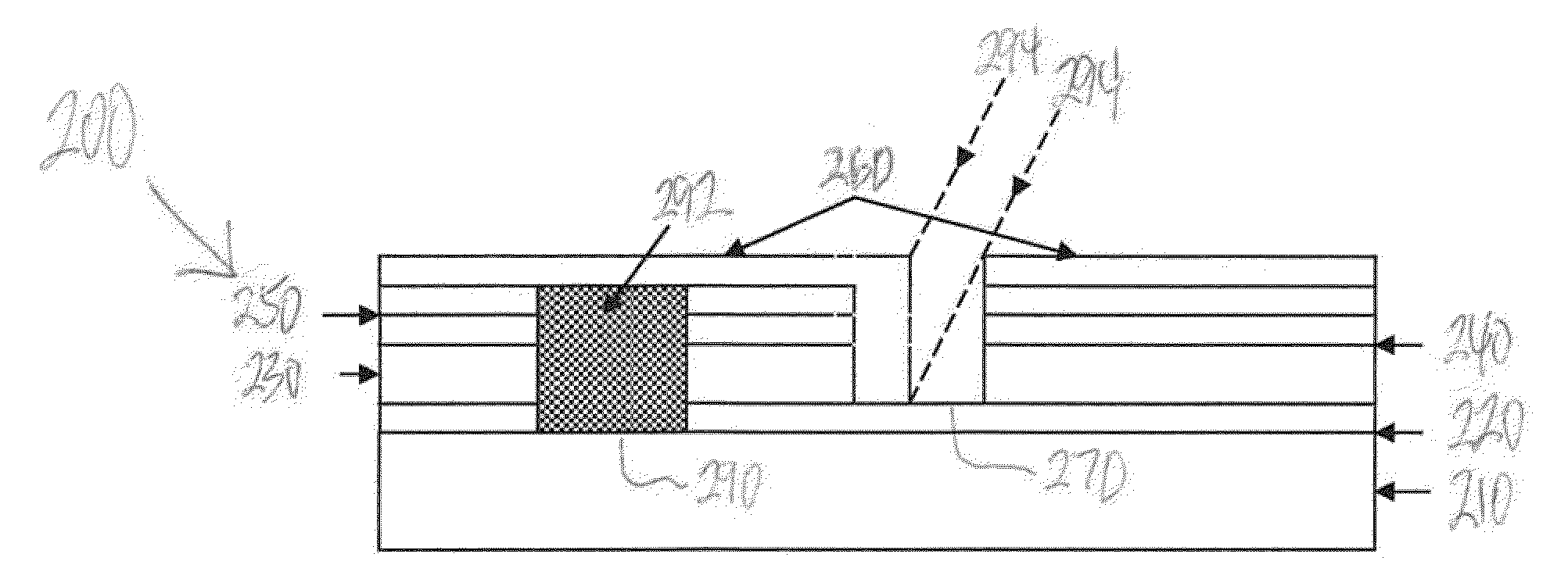
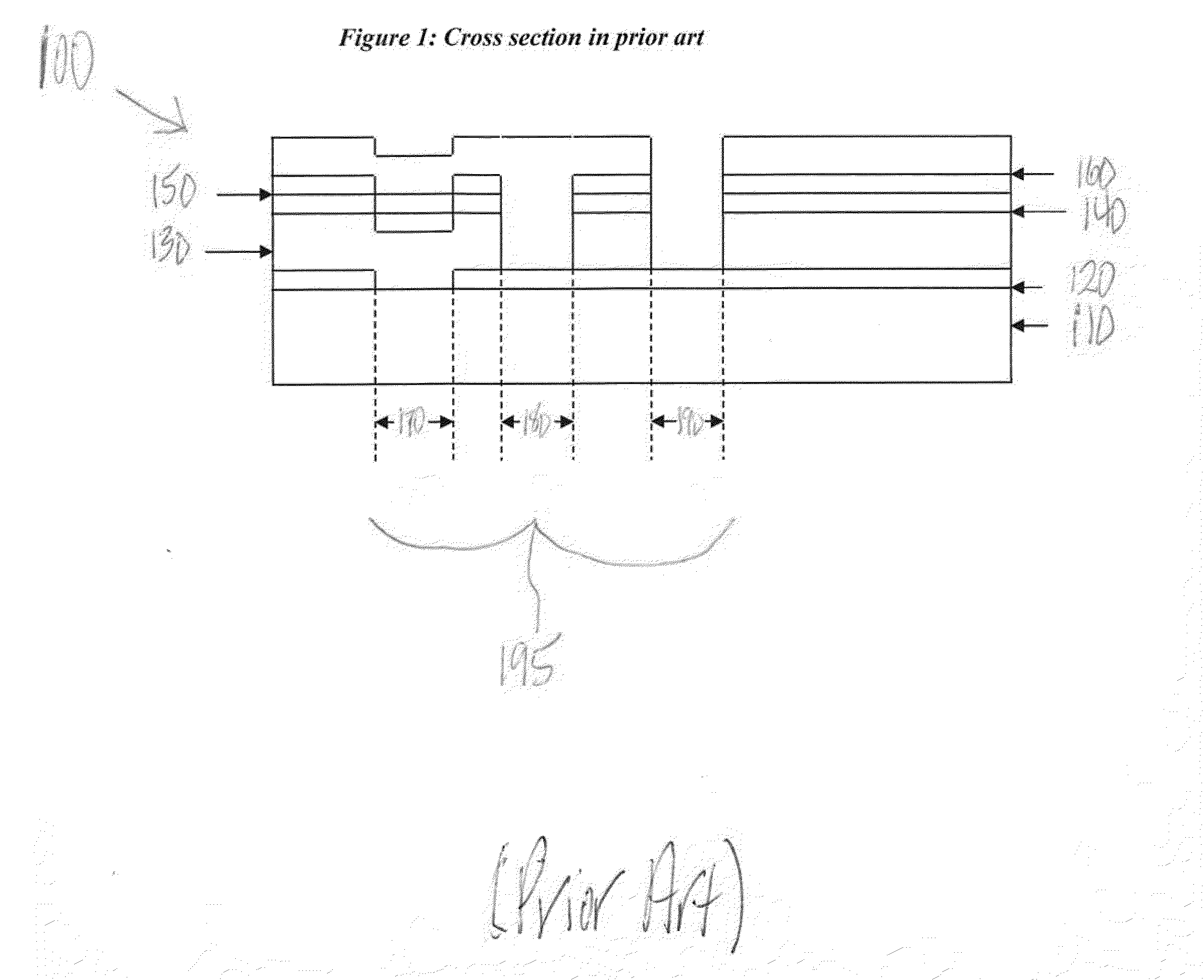
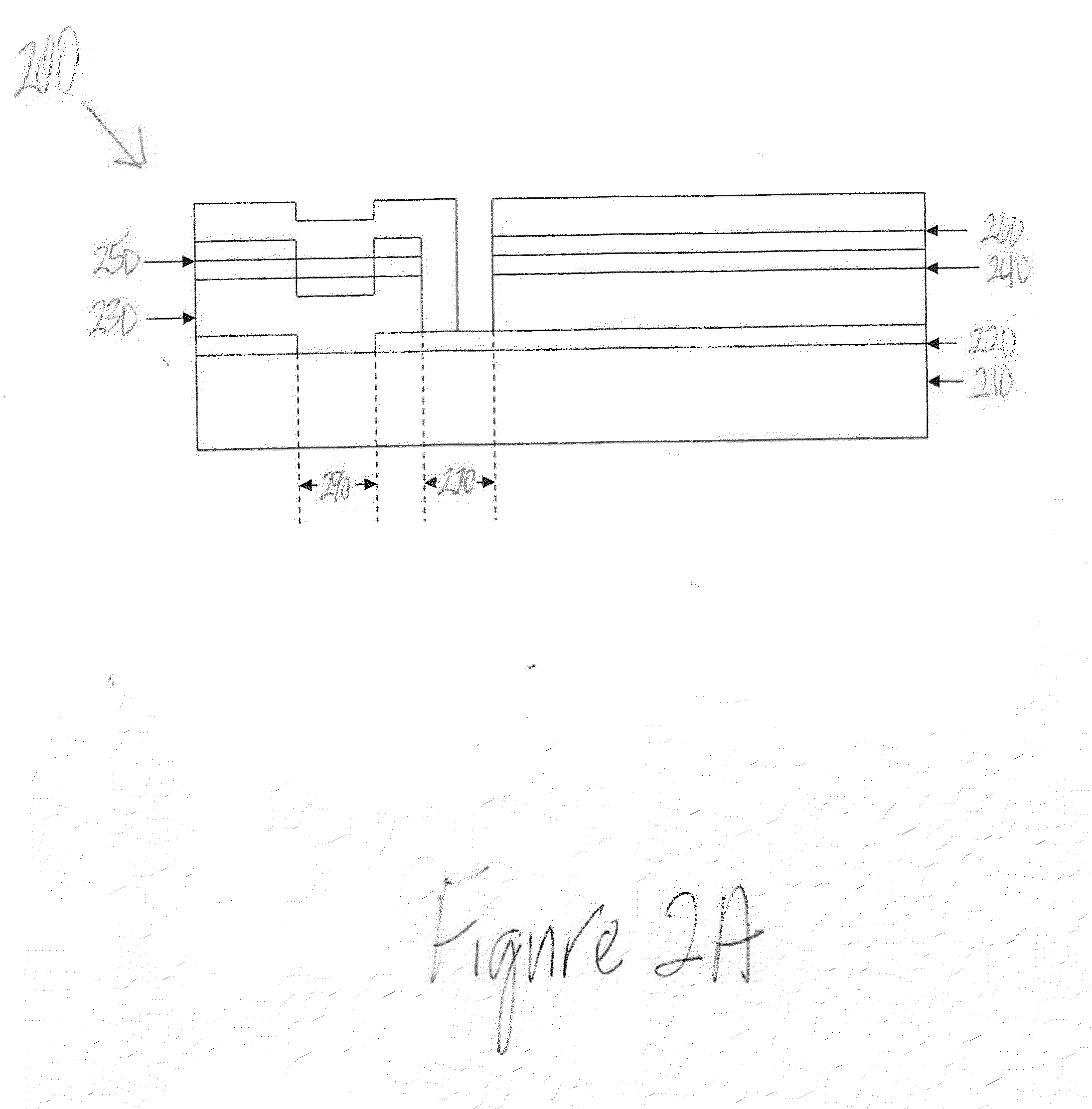
[0017]Various aspects of the illustrative embodiments will be described utilizing terms commonly employed by those skilled in the art to convey the substance of their work to others skilled in the art. However, it will be apparent to those skilled in the art that the present invention may be practiced with only some of the described aspects. For purposes of explanation, specific numbers, materials and configurations are set forth in order to provide a thorough understanding of the illustrative embodiments. However, it will be apparent to one skilled in the art that the present invention may be practiced without the specific details. In other instances, well-known features are omitted or simplified in order not to obscure the illustrative embodiments.

[0018]Various operations will be described as multiple discrete operations, in turn, in a manner that is most helpful in understanding the present invention. However, the order of description should not be construed as to imply that thes...


PUM

PropertyMeasurementUnit
Angleaaaaaaaaaa
Electrical conductoraaaaaaaaaa
Transparencyaaaaaaaaaa

Abstract

The present invention is a method for scribing a thin film solar cell that includes a soda lime glass substrate, a film of molybdenum (Mo), a film of copper indium gallium diselenide (GIGS), a buffering layer, a layer of zinc oxide (i-ZnO), a layer of aluminum doped zinc oxide (n-ZnO:Al or AZO), a first scribe, a conductive link and a second scribe. The method steps include producing the first scribe on the Mo film, depositing the CICS film, the buffering layer and the zinc oxide layer onto the Mo film, producing the second scribe on the CICS film, the zinc oxide layer and the buffering layer above the Mo film, depositing and filling a first insulating material into the first scribe. and depositing a second insulating material that covers the solar cell while filling the first scribe forming a conduction layer.

Description

[0001]This application claims priority to U.S. Provisional Application 61 / 320,319 filed on Apr. 2, 2010, the entire disclosure of which is incorporated by reference.TECHNICAL FIELD & BACKGROUND[0002]Solar cells can use thin film semiconductors to absorb sunlight and generate electron hole pairs. A p-n junction can separate out these pairs to generate electricity utilizing a bottom and a top thin film electrode. An example of this type of p-n junction involves utilizing copper indium gallium diselenide (CIGS) as an absorber, a transparent conducting oxide such as n-ZnO:Al as a negative top electrode and molybdenum (Mo) as a bottom positive electrode. Usually, each cell is connected ‘monolithically’ to its neighbor to achieve a higher output voltage utilizing a transparent conducting oxide such as n-ZnO:Al, also known as aluminum doped zinc oxide or AZO. To assemble the cell, three scribes are required, a P1 scribe, separating the Mo between each cell, a P2 scribe disposed on the CIGS...

Claims


Application Information

Patent Timeline
IPC IPC(8): H01L31/0224H01L31/0272C23C14/34
CPCH01L31/022425H01L31/022466H01L31/0322H01L31/0463H01L31/20Y02E10/541H01L31/0749H01L31/0392H01L31/022483H01L31/03923
Inventor BEATTY, PAUL HANLON JAMES
Owner BEATTY PAUL HANLON JAMES
Why Eureka
Try Eureka