Method and apparatus to scribe thin film layers of cadmium telluride solar cells

a solar cell and cadmium telluride technology, applied in the field of laser processing materials, can solve the problems of significant micro-cracking in the substrate, significant micro-cracking in the glass substrate and on the scribed edges of zno material, and achieve the effect of improving the quality of the scribing process

Inactive Publication Date: 2011-10-06
ELECTRO SCI IND INC
View PDF14 Cites 5 Cited by
  • Summary
  • Abstract
  • Description
  • Claims
  • Application Information

AI Technical Summary

Benefits of technology

[0010]The present invention relates to a method to scribe or cut a line in a thin film layer of material on a substrate using a burst of laser pulses shown schematically in FIG. 1a and consisting of individual pulses with a beneficially-formed temporal pulse shape, the use of which pulse shape instead of the conventional temporal pulse shape emitted by a laser has various advantages to improve the quality and the yield of the thin film scribing process. In one embodiment, the beneficially-shaped pulse can be described generally as a chair shape power temporal profile: an initial power spike followed by a significantly longer but lower-power plateau as shown schematically in FIG. 1b. In the scribing process where multiple pulses of the focused laser beam spot are scanned across a thin film material with some spot overlap, if a beneficially-shaped pulse of this general form is used instead of the conventional temporal pulse shape previously used, significant improvements in the quality of the scribing process are achieved. More specifically, the pulse length (FWHM full width half maximum) of each pulse in the burst of pulses is between 1 ns and 200 ns, and the pulse length FWHM of the spike is more than 0.3 ns but less than 30% of the pulse length of the full pulse. The peak power of the spike is between 1.5 times to 10 times the average peak power of the total pulse.
[0011]In another embodiment, the scribing process uses a burst of laser pulses shown schematically in FIG. 2a whereby each pulse has a beneficially-shaped pulse shape which can be described as a simple square-top pulse shape with a rapidly-rising leading edge as shown schematically in FIG. 2b. In the scribing process where multiple pulses of the focused laser beam spot are scanned across a thin film material with some spot overlap, if a beneficially-shaped pulse of this square top form is used instead of the conventional temporal pulse shape previously used, improvements in the quality of the scribing process are achieved. More specifically, the pulse length (FWHM full width half maximum) of the square pulse is between 1 ns and 200 ns.
[0012]The use of beneficial pulse shapes in the thin film scribing process has a number of advantages. For example, for laser scribing of zinc oxide thin films on a glass substrate which is a commonly-used material in solar panels, the use of the square temporal pulse shape results in no micro-cracks being generated in the glass substrate compared to the situation when a conventional laser temporal pulse shape is used which does result in significant micro-cracking in the substrate. On the same material, the use of the spike / plateau chair laser pulse shape results in no micro-cracks being generated in either the glass substrate or the scribed edges of the ZnO material compared to the situation when a conventional laser temporal pulse shape is used which results in significant micro-cracking in the glass substrate and on the scribed edges of the ZnO material. In addition, the use of the spike / plateau chair laser pulse shape also results in a significant reduction in the generation of ZnO residue and debris at the scribed line. The use of beneficial pulse shapes provides a significant improvement in the quality of the devices generated thereby and also a significant improvement in the yield as the number of devices which are acceptable to advance into the next stage of manufacturing is increased.
[0016]There are a number of designs which can be used to provide the beneficially-shaped temporal pulse shapes as desired. In a further embodiment of this invention, a materials processing system is disclosed to scribe or cut lines in a layer or layers of thin film materials on a substrate. The system includes a laser which provides a beneficially-shaped temporal pulse shape or shapes to optimally process thin film materials so as to achieve one or more of the following benefits; (1) to reduce or exclude the formation of microcracks in the substrate, (2) to reduce or exclude the formation of microcracks along the edges of the thin film cut region, (3) to reduce debris formation, and (4) to reduce surface area residue. As well as the laser, the materials processing system includes means to focus, image and scan the laser beam in a line across the thin film material so as to perform the scribing process, means to adjust the overlap of the scanned laser spot, and a computer to control the process. In a related embodiment, the materials processing system may also include means to change the wavelength of the laser using the process of harmonic generation.

Problems solved by technology

For example, for laser scribing of zinc oxide thin films on a glass substrate which is a commonly-used material in solar panels, the use of the square temporal pulse shape results in no micro-cracks being generated in the glass substrate compared to the situation when a conventional laser temporal pulse shape is used which does result in significant micro-cracking in the substrate.
On the same material, the use of the spike / plateau chair laser pulse shape results in no micro-cracks being generated in either the glass substrate or the scribed edges of the ZnO material compared to the situation when a conventional laser temporal pulse shape is used which results in significant micro-cracking in the glass substrate and on the scribed edges of the ZnO material.

Method used


Image

  • Method and apparatus to scribe thin film layers of cadmium telluride solar cells
  • Method and apparatus to scribe thin film layers of cadmium telluride solar cells
  • Method and apparatus to scribe thin film layers of cadmium telluride solar cells

Examples


Embodiment Construction

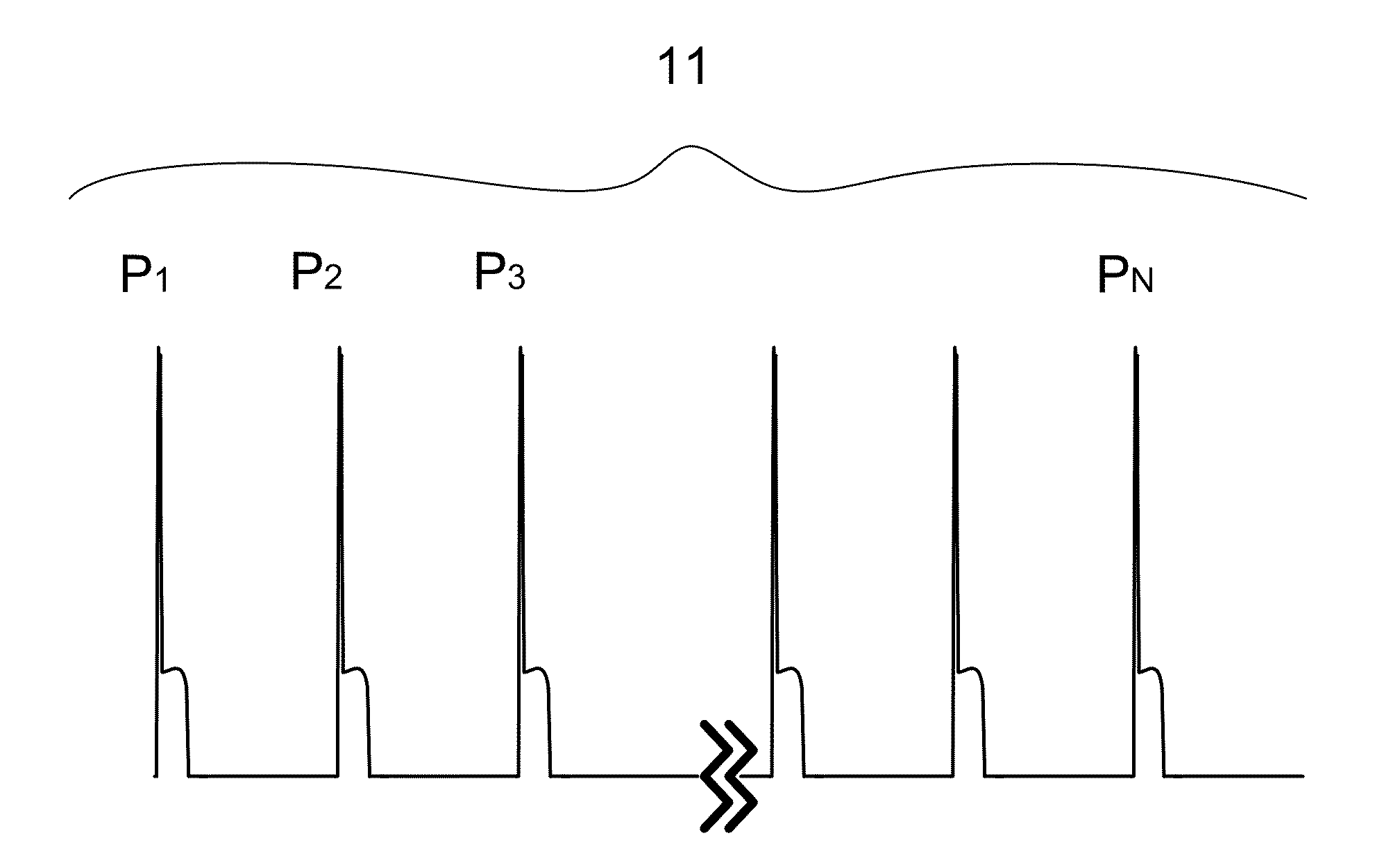
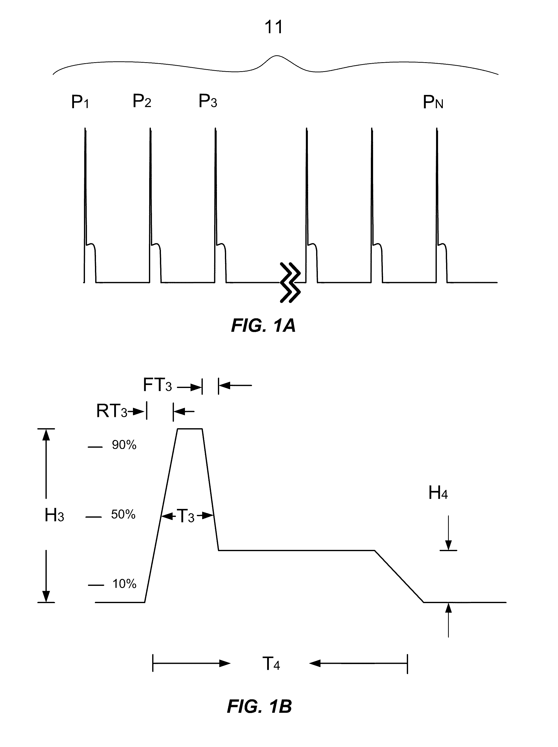
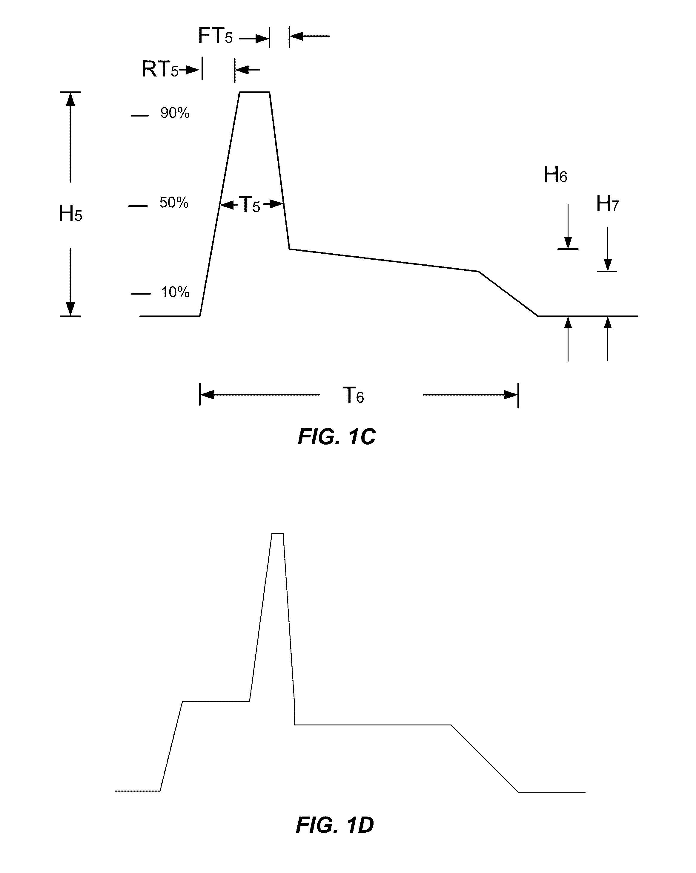
[0040]In the manufacturing process of solar cells, flat panel displays, and digital displays, a thin film of a transparent conducting oxide (TCO) material deposited on a glass substrate must be segmented by scribing lines in the TCO material, thereby segmenting to provide electrical isolation between the TCO segment on one side of the line and the TCO segment on the other side of the line. Scribing a line using a pulsed laser is a multiple pulse process using a burst of many laser pulses whereby each pulse is focused to a spot on the thin film and the spot is scanned along the desired line to be scribed such that there is some overlap between each spot with the previous spot and the following spot. The width of the scribed line is determined primarily by the size of the focused laser spot. Widths for lines are scribed in a ZnO thin film on a glass substrate range from 10 microns to 100 microns although even thinner lines can be achieved. A certain amount of spot overlap is used to a...


PUM

PropertyMeasurementUnit
thicknessaaaaaaaaaa
thicknessaaaaaaaaaa
peak power levelaaaaaaaaaa

Abstract

A method of laser scribing a CdTe solar cell structure includes providing a laser operable to produce an optical pulse. The optical pulse is characterized by a temporal profile having a first power level during a first portion of the optical pulse and a second power level less than the first power level during a second portion of the optical pulse. The method also includes directing the optical pulse to impinge on the CdTe solar cell structure. The CdTe solar cell structure includes a substrate, a transmission spectrum control layer adjacent the substrate; a barrier layer adjacent the transmission spectrum control layer, and a conductive layer adjacent the barrier layer. The method further includes initiating a removal process for the conductive layer and terminating the removal process prior to removing the insulating layer.

Description

CROSS-REFERENCES TO RELATED APPLICATIONS[0001]This application is a continuation-in-part of U.S. patent application Ser. No. 12 / 889,435, filed on Sep. 24, 2010, entitled “Method and Apparatus to Scribe a Line in a Thin Film Material Using a Burst of Laser Pulses With Beneficial Pulse Shape,” which claims priority to U.S. Provisional Patent Application No. 61 / 245,582, filed on Sep. 24, 2009, entitled “Method and Apparatus to Scribe a Line in a Thin Film Material Using a Burst of Laser Pulses With Beneficial Pulse Shape,” the disclosures of which are hereby incorporated by reference in their entirety for all purposes.BACKGROUND OF THE INVENTION[0002]The present invention relates generally to laser processing of materials. More particularly, the present invention relates to methods and apparatus employing a series of laser pulses which have been specifically shaped to provide better processing quality and higher throughput in laser processing applications. The present invention also re...

Claims


Application Information

Patent Timeline
Patent Type & Authority Applications(United States)
IPC IPC(8): B23K26/38
CPCB23K26/0635B23K26/409B23K26/367B23K26/365B23K26/40B23K26/0624B23K26/361B23K26/364B23K2103/172
Inventor PANARELLO, TULLIOREKOW, MATHEWMURISON, RICHARD
Owner ELECTRO SCI IND INC
Why Eureka
Try Eureka