[0016]The present invention will now be described more fully hereinafter with reference to the accompanying drawings, in which preferred embodiments of the invention are shown. This invention, however, may be embodied in many different forms and should not be construed as limited to the embodiments set forth herein. Rather, these embodiments are provided so that this disclosure will be thorough and complete, and will fully convey the scope of the invention to those skilled in the art. In the drawings, like numbers refer to like elements throughout.
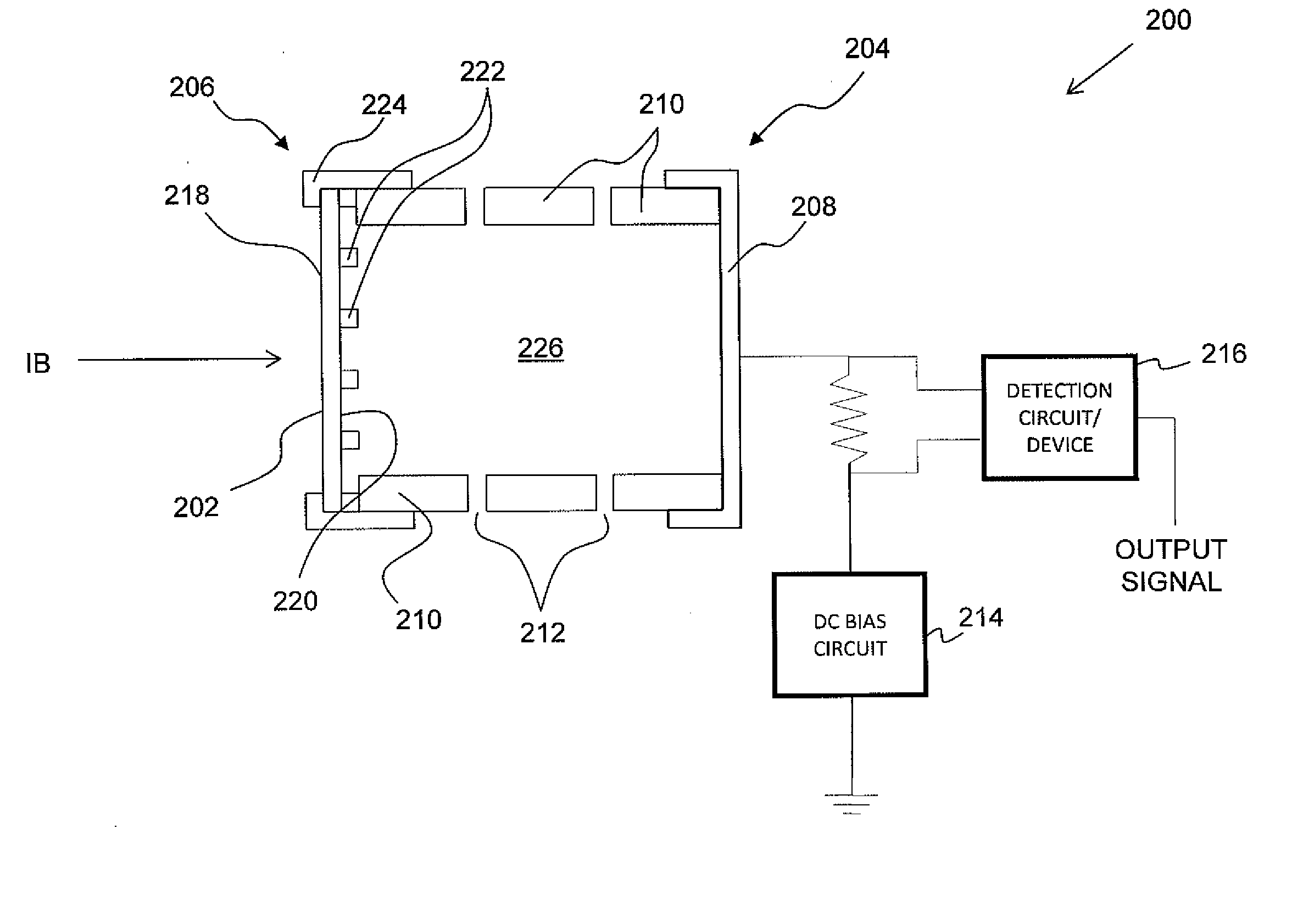
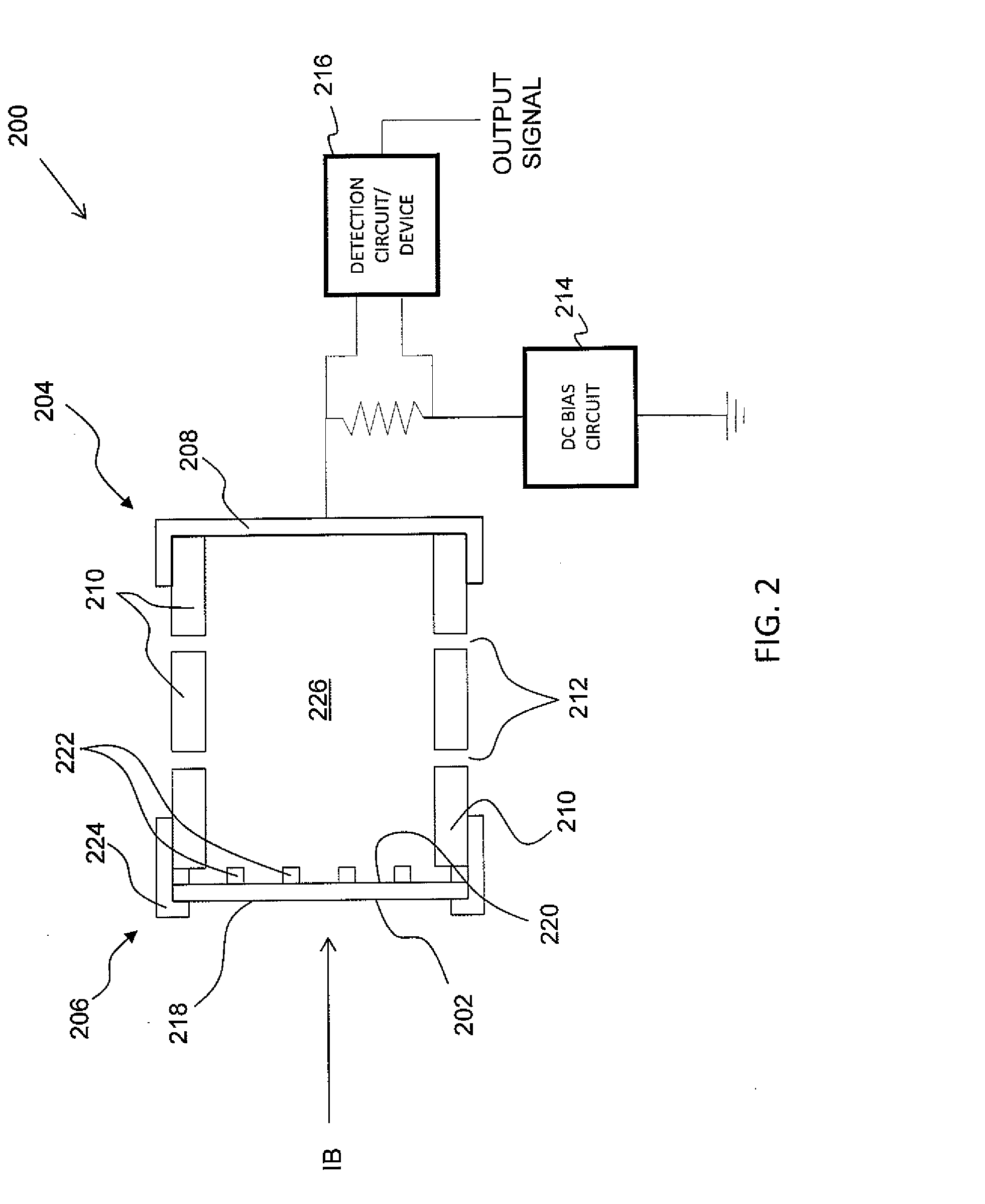
[0017]FIG. 2 is a block diagram of an exemplary energy contamination (EC) detector 200, which may be disposed on or near platen 114 of an ion implanter 100. In particular, the detector 200 may replace a target substrate in situ to obtain the desired implant processing parameters. Once the desired parameters are achieved, the detector 200 is removed from or near the platen and replaced by the target substrate. EC detector 200 includes a membrane 202 supported by a housing 204 including a support frame 206. The housing 204 defines an interior chamber 226. A charge collection plate 208 is separated from membrane 202 by insulators 210 defining one or more pumping holes 212 therebetween. Charge collection plate 208 is coupled to a direct current (DC) bias circuit 214 and to a detection circuit or device 216.
[0018]Support frame 206 of housing 204 is configured to support membrane 202. When EC detection device 200 is positioned on or near platen 114, membrane 202 receives ion beam 250 comprised of ions and neutrals. Support frame 206 may include a grid 222 for providing a backing to membrane 202, and clamps 224 or other mounting device may be used to releasably secure membrane 202 to grid 222. Membrane 202 receives the ion beam 250 and only allows the portion of the beam having high energy particles (EC) to emerge on the downstream side of membrane 202. These particles may emerge as ions or neutrals that release secondary electrons which provides a detectable signal at collection plate 208 as described below. The energy particles that form beam 250 that are not part of the EC particles (i.e. the ions at or below the desired lower energy level for shallow implantation) are prevented from emerging from surface 220 and are essentially “filtered” out by membrane 202. Thus, only the high energy contaminating particles emerge from the surface 220 of membrane 202 and can be measured directly without any numerical subtraction.
[0019]As mentioned above, prior attempts at EC detection required the measuring of the various components of the beam current including, for example, the total beam and the desired energy level ions and then inferring the EC by subtracting these two quantities. In contrast, in the present disclosure the role of the subtraction operation is substituted by the physical filtering of the EC particles in the membrane.
[0020]The thickness of membrane 202 may be selected based on an energy of the desired ion beam 250 for a specific implant recipe for fabricating devices on a substrate or wafer. For example, membrane 202 may have a thickness of approximately 30 nm for detecting EC in a semiconductor fabrication process using an ion beam having an energy of approximately 300 keV, and a thickness of approximately 15 nm for detecting EC for a recipe using a 150 keV process. Membrane 202 may be a diamond-like carbon (DLC) foil such as those available from Micromatter of Vancouver, British Columbia, Canada. Membranes 202 may be fabricated from other similar materials and have a thickness between approximately 10 nm and approximately 600 nm. However, membranes 202 having other thicknesses may also be implemented.
[0021]Charge collection plate 208 is fabricated from a conductive material and is electrically separated from support frame 206 by insulating walls 210. This enables a DC bias to be applied to collection plate 208 without being applied to membrane 202. Insulating sidewalls 210 may be formed from any substantially non-conductive material. One or more holes 212 enables interior chamber 226 of EC detection device 200 to be pumped with gas for equilibrating the pressure or the gas concentration within the chamber. Alternatively, holes 212 may be used to create a vacuum within chamber 226. Holes 212 also enable the gas composition and pressure in the interior chamber 226 of EC detection device 200 to provide a consistent proportional electron gain. For very small amounts of EC, a higher DC bias may be applied to operate in an avalanche or Geiger counter mode and count individual high energy ions.
[0022]Detection circuit or device 216 may be any circuit or device configured to detect a voltage or current on charge collection plate 208. In one embodiment, detection device 216 is a nanoammeter such as, for example, a Model 285 nanoammeter available from Monroe Electronics of Lyndonville, N.Y.
[0023]In operation, a membrane 202 is loaded onto housing 204 of EC detection device 200. As described above, the thickness of membrane 202 is selected based on a desired ion beam energy in a recipe for fabricating devices on a target substrate. The EC device 200 is positioned on platen 114 of ion implanter 100 in the position in which a target substrate is to be positioned during the fabrication process. The EC detector 200 and in particular housing 204, has a sufficient size to receive at least a portion of incident ion beam 250. Obviously, the size of detector 200 is such that it fits within the confines of a processing chamber of ion implanter 100. Once EC device 200 is positioned on platen 114, an ion bean 250 is incident on membrane 202.
[0024]Membrane 202 absorbs or deflects ions having an appropriate energy for the semiconductor fabrication recipe. Only the EC particles, which may be ions or neutrals, emerge from the downstream surface 220 of membrane 202 toward charge collection plate 208. Some of these high energy particles will be ionized as their remaining kinetic energy is greater than the electron binding energy. These ions are collected via collection plate 208 by applying a relatively small DC bias to the collection plate with DC bias circuit 214. For example, ions may be collected by providing a negative DC bias (e.g., 10-50V) to charge collection plate 208. Alternatively, as the EC particles emerge from the downstream surface 220 of membrane 202, they may be negatively charged ions or secondary electrons which are generated by the neutrals. These negatively charged particles may be collected by applying a positive DC bias to charge collection plate 208. Larger DC biases may be applied to induce electron multiplication in the residual gas in order to increase the collected current above a threshold level associated with these secondary electrons.
[0025]As charge accumulates on charge collection plate 208, a measurable signal (e.g., voltage or current) develops on collection plate 208. For example, a typical high current ion beam has a current density of approximately 100 μA/cm2, and a typical maximum EC requirement for a semiconductor wafer is approximately 0.1%. Accordingly, the detection device 216 of EC detection device 200 having a membrane 202 with an area of approximately 1 cm2 may measure a current of approximately 100 nA, which identifies the presence of EC contamination. Consequently, an operator may adjust the settings of ion implanter 100, replace membrane 202, and have ion implanter 100 transmit another ion beam towards membrane 202 to test for energy contamination.
[0026]If a current or voltage above a threshold is not detected by detection device 216, then the ion implanter 100 is properly calibrated for fabricating devices on the semiconductor wafer according to the recipe for which the EC detection was performed. Accordingly, the ion implanter 100 may then be used to fabricate devices on semiconductor wafers with a lower risk of energy contamination.
[0027]While the present invention has been disclosed with reference to certain embodiments, numerous modifications, alterations and changes to the described embodiments are possible without departing from the sphere and scope of the present invention, as defined in the appended claims. Accordingly, it is intended that the present invention not be limited to the described embodiments, but that it has the full scope defined by the language of the following claims, and equivalents thereof.