Avalanche photodiode

a photodiode and avalanche technology, applied in the field of avalanche photodiodes, can solve the problems of poor element manufacturing yield, inability to reach, and difficult to precisely control the zn heat diffusion, and achieve the effect of suppressing edge breakdown without highly precise control

Active Publication Date: 2011-10-06
NTT ELECTORNICS CORP +1
View PDF5 Cites 7 Cited by
  • Summary
  • Abstract
  • Description
  • Claims
  • Application Information

AI Technical Summary

Benefits of technology

[0023]The present disclosure can provide an electron injection-type APD that uses an embedded n electrode structure as a base and can s

Problems solved by technology

However, it is a serious and technical problem that precise control of the Zn heat diffusion is difficult, and an element manufacturing yield is generally poor.
A problem of the electron injection-type APD is that a so-called “guard ring technology” for suppressing edge breakdown around a junction does not reach to completeness in the hole injected APD.
This is because it is difficult in the electron injection-type APD to form an “ion implated guard ring structure” generally used by the hole injected APD, that is, a structure to adjust a depth distribution of acceptor ions such as Be and decrease a multiplication coefficient (increase a breakdown voltage).
This structure is effective in the elect

Method used


Image

  • Avalanche photodiode
  • Avalanche photodiode
  • Avalanche photodiode

Examples


first embodiment

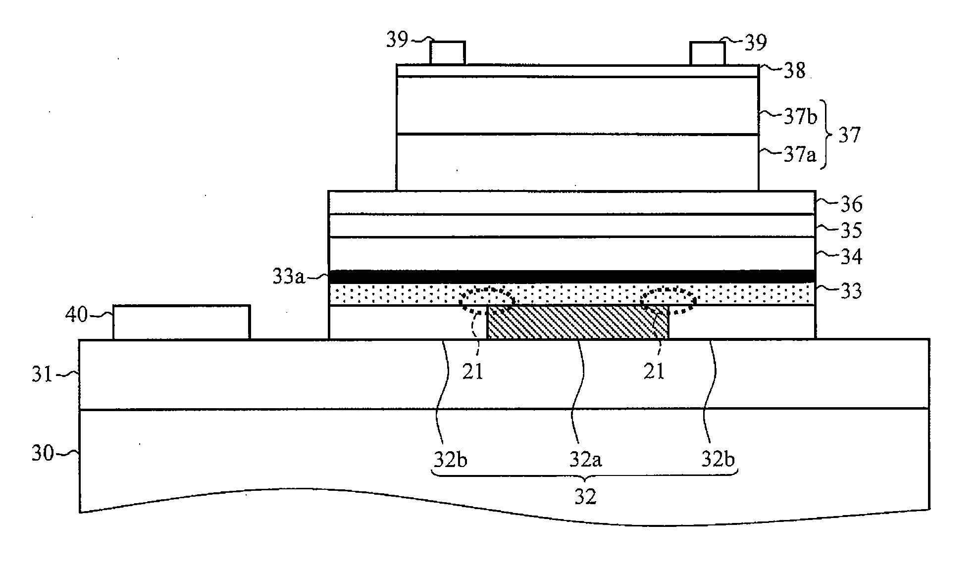
[0031]FIG. 1 is a schematic view of a device element cross-section illustrating an APD according to a first embodiment. The APD of FIG. 1 is an electron injection-type APD in which an n electrode layer 31, an n electrode connecting layer 32, a buffer layer 33, an avalanche multiplication layer 34, an electric field control layer 35, a band gap gradient layer 36, a low-concentration light absorbing layer 37a, a p-type light absorbing layer 37b, and a p electrode layer 38 are sequentially stacked, and a light absorbing portion 37 including at least the low-concentration light absorbing layer 37a and the p-type light absorbing layer 37b forms a mesa shape. The APD of FIG. 1 adopts an embedded n electrode structure in which the n electrode connecting layer 32 has an n-type region 32a that is disposed to be closer to the inner side than the periphery of the avalanche multiplication layer 34 and the periphery of the mesa of the light absorbing portion 37, when viewed from a stack directio...

second embodiment

[0037]FIG. 3 is a schematic view of a device element cross-section illustrating an APD according to a second embodiment. The APD of FIG. 3 is also an electron injection-type APD that adopts the embedded n electrode structure, similar to the APD of FIG. 1. The difference of the APD of FIG. 3 and the APD of FIG. 1 is that the doping portion 33a does not need to be formed in the buffer layer 33 of the APD of FIG. 3, the APD is a semiconductor with a composition different from a composition of each of the buffer layer 33 and the avalanche multiplication layer 34, and the buffer layer 33 has a band gap wider than a band gap of the avalanche multiplication layer 34.

[0038]The composition of each layer from the n electrode layer 31 to the buffer layer 33 is the same as the composition of the APD of FIG. 1. The avalanche multiplication layer 34 is InAlGaAs that has a low doping concentration. The electric field control layer 35 is p-InAlGaAs. The band gap gradient layer 36 is an InAlGaAs lay...

third embodiment

[0041]FIG. 5 is a schematic view of a device element cross-section illustrating an APD according to a third embodiment. The p electrode layer 38, the p-type light absorbing layer 37b, the low-concentration light absorbing layer 37a, the band gap gradient layer 36, the electric field control layer 35, the avalanche multiplication layer 34, the buffer layer 33, the n electrode connecting layer 32, and the n electrode layer 31 are sequentially stacked on the substrate 30, and the p electrode 39 and the n electrode 40 are formed. This structure corresponds to the case where the semiconductor structure according to the second embodiment is vertically reversed. In this case, since the n electrode connecting layer 32 exists in an upper portion, instead of the substrate side, formation of the n layer by the injection of the Si ions in the cases of the first and second embodiments is not needed, and the mesa shape may be simply determined. That is, by disposing the n electrode connecting lay...


PUM


Abstract

An electron injected APD with an embedded n electrode structure in which edge breakdown can be suppressed without controlling the doping profile of an n-type region of the embedded n electrode structure with high precision. The APD comprising a buffer layer with a low ionization rate is inserted between an n electrode connecting layer and an avalanche multiplication layer. Specifically, the APD is an electron injected APD in which an n electrode layer, the n electrode connecting layer, the buffer layer, the avalanche multiplication layer, an electric field control layer, a band gap gradient layer, a low-concentration light absorbing layer, a p-type light absorbing layer, and a p electrode layer are sequentially stacked, and a light absorbing portion that includes at least the low-concentration light absorbing layer and the p-type light absorbing layer forms a mesa shape.

Description

BACKGROUND[0001]1. Field of the Disclosure[0002]The present disclosure relates to a device element structure of an electron injection-type avalanche photodiode (photodiode with avalanche multiplication function: hereinafter, simply referred to as APD) that is suitable for a ultra-high speed operation.[0003]2. Discussion of the Background Art[0004]The APD that functions as a Photoreceiver device with high sensitivity is widely introduced in a 10 Gb / s system and the like that uses a long wavelength range (1.5 microns). The typical APD that operates in the long wavelength range is a hole injected APD that uses InP as an avalanche multiplication layer. Almost all the hole injected APDs take a manufacturing process that defines an avalanche multiplication region by Zn heat diffusion to InP. However, it is a serious and technical problem that precise control of the Zn heat diffusion is difficult, and an element manufacturing yield is generally poor.[0005]Meanwhile, an electron injection-t...

Claims


Application Information

Patent Timeline
IPC IPC(8): H01L31/0224
CPCH01L31/1075
Inventor ISHIBASHI, TADAOANDO, SEIGOMURAMOTO, YOSHIFUMINAKAJIMA, FUMITOYOKOYAMA, HARUKI
Owner NTT ELECTORNICS CORP
Why Eureka
Try Eureka