Uncooled infrared detector and methods for manufacturing the same

a technology of infrared detectors and manufacturing methods, applied in the field of infrared detectors, can solve the problems of high rate of high precision lithography, low yield of customer-specific fabrication processes, and high cost, and achieve the effects of reducing time and cost, cost efficiency, and convenient operation

Active Publication Date: 2011-10-13
MIKROSENS ELEKTRONIK SAN & TIC A S
View PDF1 Cites 32 Cited by
  • Summary
  • Abstract
  • Description
  • Claims
  • Application Information

AI Technical Summary

Benefits of technology

[0011]The generic SOI-CMOS process may be defined and offered by one or more foundries (e.g., fabrication companies that fabricate SOI-CMOS wafers). The generic SOI-CMOS process may fulfill the design requirements of many customers. As such, the generic SOI-CMOS process typically involves standard design rules, process sequence, and / or process parameters, which may reduce the time and cost for fabricating the foundry-defined SOI-CMOS wafers. Moreover, because of its standardization nature, the SOI-CMOS wafers fabricated according to the generic SOI-CMOS process can be adopted by other applications. Due to the economies of scale, the production cost of foundry-defined SOI-CMOS wafers (a.k.a. standard SOI-CMOS wafers) can be substantially reduced.
[0012]The manufacturing methods disclosed herein involve a few process steps for modifying the foundry-defined SOI-CMOS wafers. The modification may allow the SOI-CMOS wafers to incorporate the functional and structural features of the uncooled infrared detectors. When compared to conventional lithography and deposition steps, these process steps may be cost efficient and easy to perform because they have a relatively high tolerance margin (a.k.a. non-critical). Advantageously, the methods disclosed herein may allow the cost and yield of the uncooled infrared detectors to be improved tremendously.
[0013]In one embodiment, the present invention may be a silicon-on-insulator (SOI) complementary metal oxide semiconductor (CMOS) wafer for use in manufacturing an uncooled microbolometer. The SOI-CMOS wafer may include a substrate layer, an insulation layer formed on the substrate layer, the insulation layer having a pixel region and a wall region surrounding the pixel region, a pixel structure formed on the pixel region of the insulation layer, a wall structure formed adjacent to the pixel structure and on the wall region of the insulation layer, a dielectric layer covering the pixel structure and the wall structure, a pixel mask formed within the dielectric layer, and for protecting the pixel structure during a dry etching process, and a wall mask formed within the dielectric layer, and for protecting the wall structure during the dry etching process, thereby releasing a space defined between the wall structure and the pixel structure after the dry etching process.

Problems solved by technology

However, these customer-specific fabrication processes generally involve several iterations of high precision lithography, each of which may be costly and time consuming to perform.
Moreover, these customer-specific fabrication processes may suffer from low yield because the failure rates of high precision lithography are statistically high.
In exchange for a better yield, some conventional infrared detectors may sacrifice the reliability of the pixels, the closed wells, and / or the support structures.

Method used


Image

  • Uncooled infrared detector and methods for manufacturing the same
  • Uncooled infrared detector and methods for manufacturing the same
  • Uncooled infrared detector and methods for manufacturing the same

Examples


Embodiment Construction

[0028]Apparatus, systems and methods that implement the embodiment of the various features of the present invention will now be described with reference to the drawings. The drawings and the associated descriptions are provided to illustrate some embodiments of the present invention and not to limit the scope of the present invention. Throughout the drawings, reference numbers are re-used to indicate correspondence between reference elements. In addition, the first digit of each reference number indicates the figure in which the element first appears.

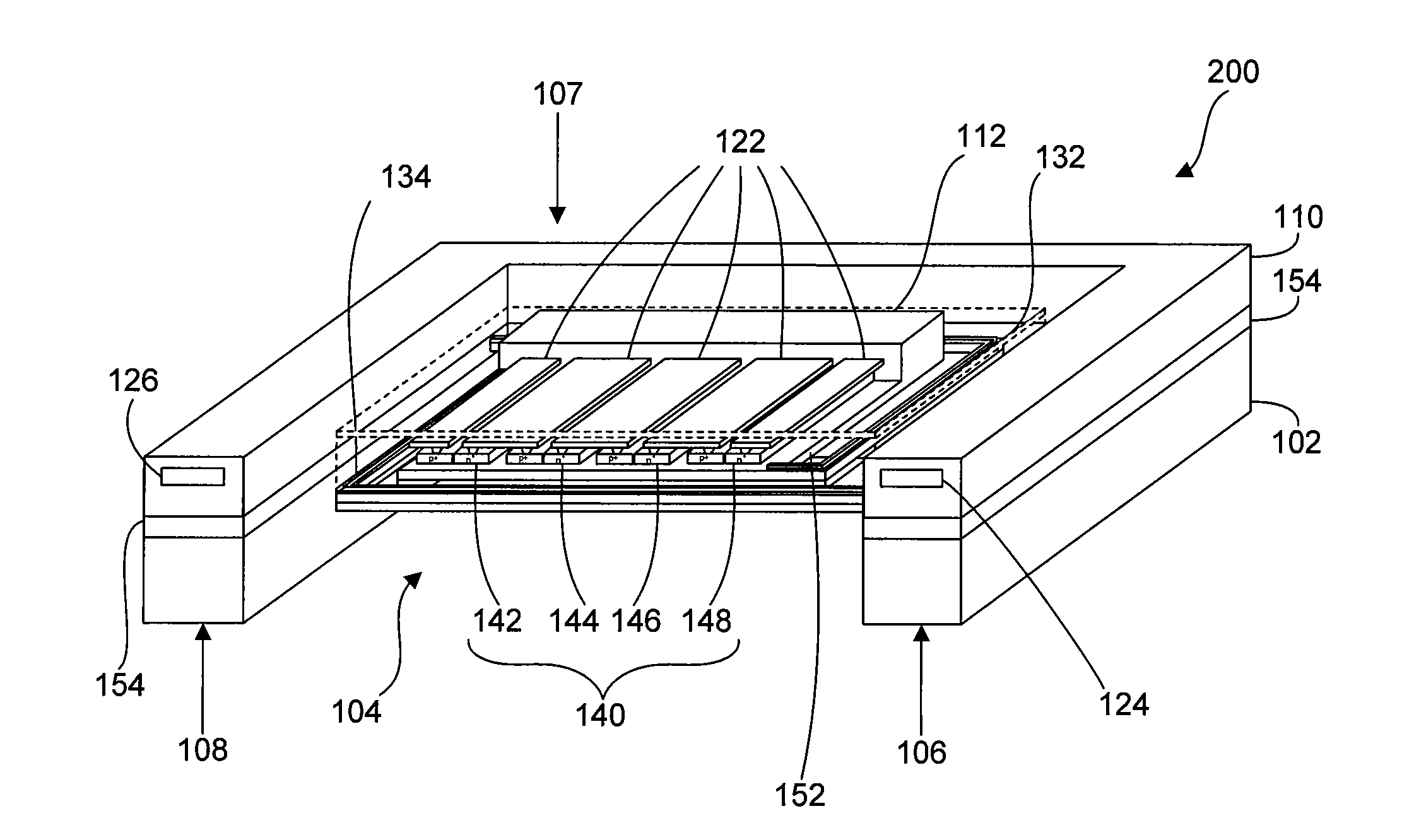
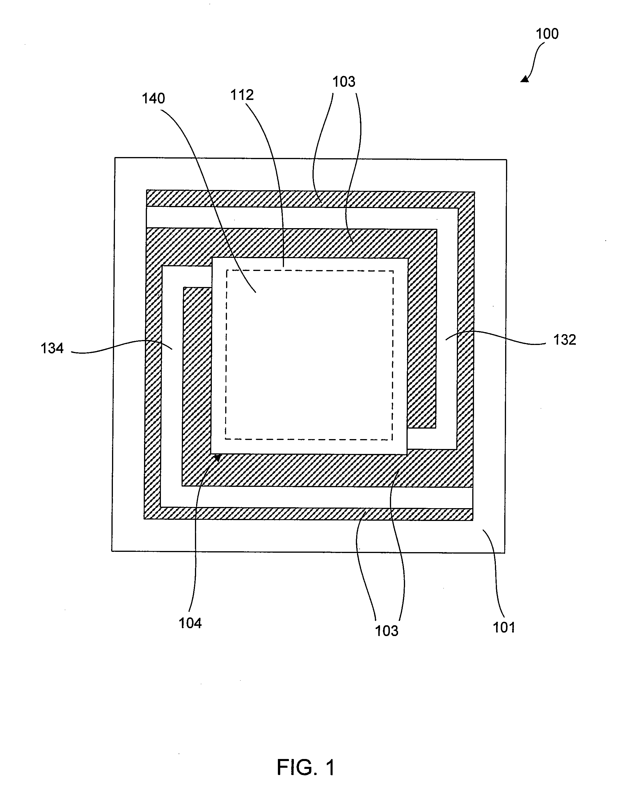
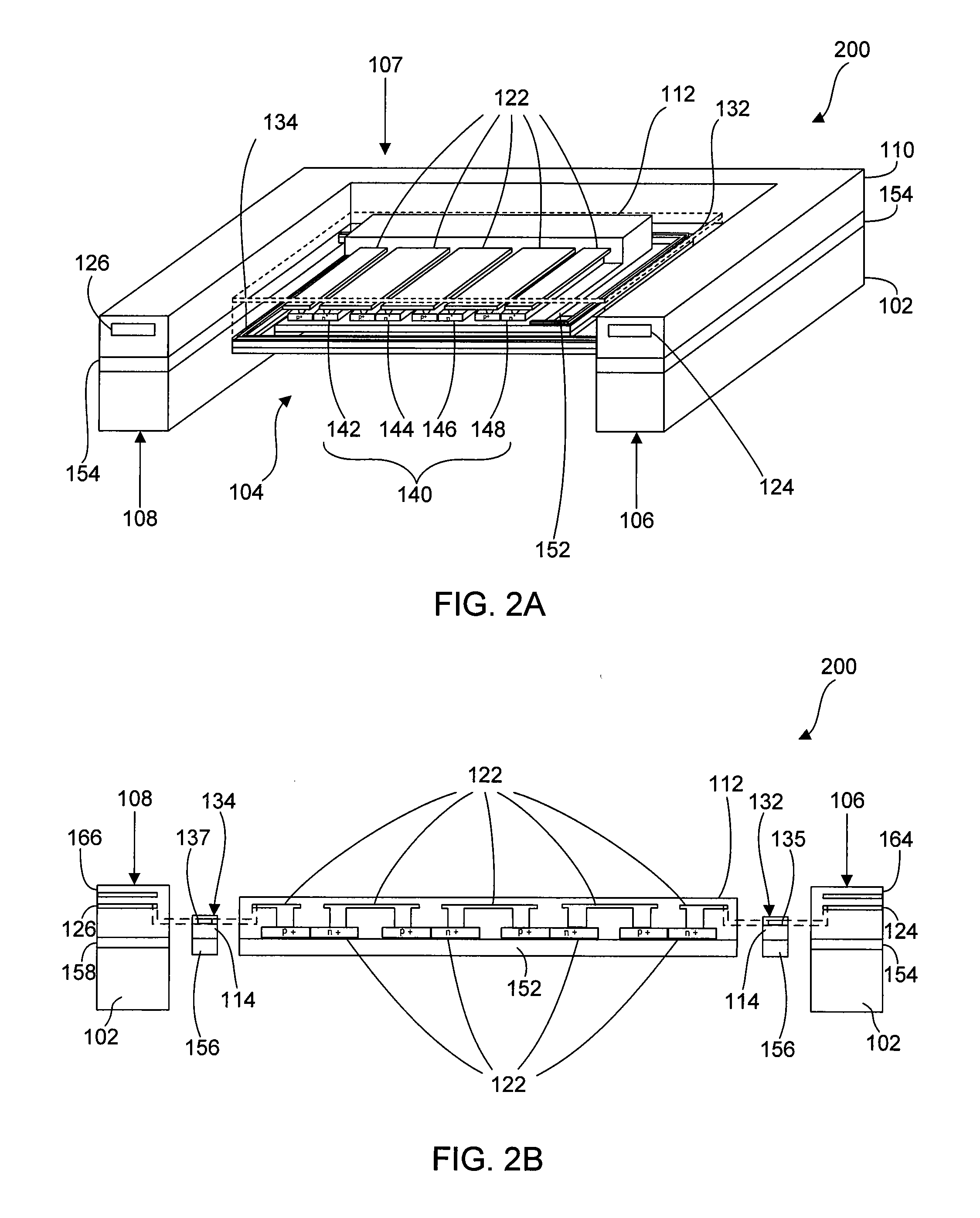
[0029]FIG. 1 shows a top view of an infrared detector pixel 100 according to an embodiment of the present invention. The infrared detector pixel 100 may be a single sensing unit, such that it may be duplicated and arranged to form a microbolometer focal plane array (FPA). The infrared detector pixel 100 may include a pixel wall 101, a pixel island 104, a first (right) support arm 132, and a second (left) support arm 134.

[0030]The pixel ...


PUM


Abstract

This disclosure discusses various methods for manufacturing uncooled infrared detectors by using foundry-defined silicon-on-insulator (SOI) complementary metal oxide semiconductor (CMOS) wafers, each of which may include a substrate layer, an insulation layer having a pixel region and a wall region surrounding the pixel region, a pixel structure formed on the pixel region of the insulation layer, a wall structure formed adjacent to the pixel structure and on the wall region of the insulation layer, a dielectric layer covering the pixel structure and the wall structure, a pixel mask formed within the dielectric layer and for protecting the pixel structure during a dry etching process, and a wall mask formed within the dielectric layer and for protecting the wall structure during the dry etching process, thereby releasing a space defined between the wall structure and the pixel structure after the dry etching process.

Description

CROSS REFERENCE TO RELATED APPLICATION[0001]This application claims priority to and the benefit of U.S. Provisional Application No. 61 / 322,982, entitled “UNCOOLED INFRARED DETECTOR ARRAYS AND METHODS FOR MANUFACTURE,” filed on Apr. 12, 2010, which is assigned to the assignee hereof and hereby expressly incorporated by reference herein.BACKGROUND[0002]1. Field[0003]The present invention generally relates to the field of infrared detectors, and more particularly to uncooled infrared detectors that are manufactured from foundry-defined silicon-on-insulator (SOI) complementary metal oxide semiconductor (CMOS) wafers.[0004]2. Description of the Related Art[0005]An uncooled (thermal) infrared detector is a device including a pixel with an infrared absorption layer (a.k.a. heat absorption layer) and a thermoelectric conversion element. The infrared absorption layer receives and converts an infrared ray (wave) into heat. The thermoelectric conversion element converts the heat into an electr...

Claims


Application Information

Patent Timeline
Patent Type & Authority Applications(United States)
IPC IPC(8): H01L29/66H01L21/308
CPCG01J5/20G01J5/024H01L27/14669H01L27/14683H01L27/1203H01L27/14
Inventor AKIN, TAYFUNEMINOGLU, SELIM
Owner MIKROSENS ELEKTRONIK SAN & TIC A S
Why Eureka
Try Eureka